- 您現(xiàn)在的位置:買賣IC網(wǎng) > PDF目錄360864 > INA2126UAG4 Micropower single-supply CMOS Instrumentation Amplifier PDF資料下載
參數(shù)資料
| 型號: | INA2126UAG4 |
| 元件分類: | 測量放大器 |
| 英文描述: | Micropower single-supply CMOS Instrumentation Amplifier |
| 中文描述: | 微功耗單電源 CMOS 儀表放大器 |
| 文件頁數(shù): | 7/19頁 |
| 文件大?。?/td> | 1368K |
| 代理商: | INA2126UAG4 |
INA126, INA2126
SBOS062A
7
www.ti.com
APPLICATION INFORMATION
Figure 1 shows the basic connections required for operation
of the INA126. Applications with noisy or high impedance
power supplies may require decoupling capacitors close to
the device pins as shown.
The output is referred to the output reference (Ref) terminal
which is normally grounded. This must be a low-impedance
connection to ensure good common-mode rejection. A resis-
tance of 8
in series with the Ref pin will cause a typical
device to degrade to approximately 80dB CMR.
Dual versions (INA2126) have feedback sense connections,
Sense
A
and Sense
B
. These must be connected to their respec-
tive output terminals for proper operation. The sense con-
nection can be used to sense the output voltage directly at the
load for best accuracy.
SETTING THE GAIN
Gain is set by connecting an external resistor, R
G
, as shown:
(1)
Commonly used gains and R
G
resistor values are shown in
Figure 1.
The 80k
term in equation 1 comes from the internal metal film
resistors which are laser trimmed to accurate absolute values.
The accuracy and temperature coefficient of these resistors are
included in the gain accuracy and drift specifications.
The stability and temperature drift of the external gain
setting resistor, R
G
, also affects gain. R
G
’s contribution to
gain accuracy and drift can be directly inferred from the gain
equation (1). Low resistor values required for high gain can
make wiring resistance important. Sockets add to the wiring
resistance, which will contribute additional gain error in
gains of approximately 100 or greater.
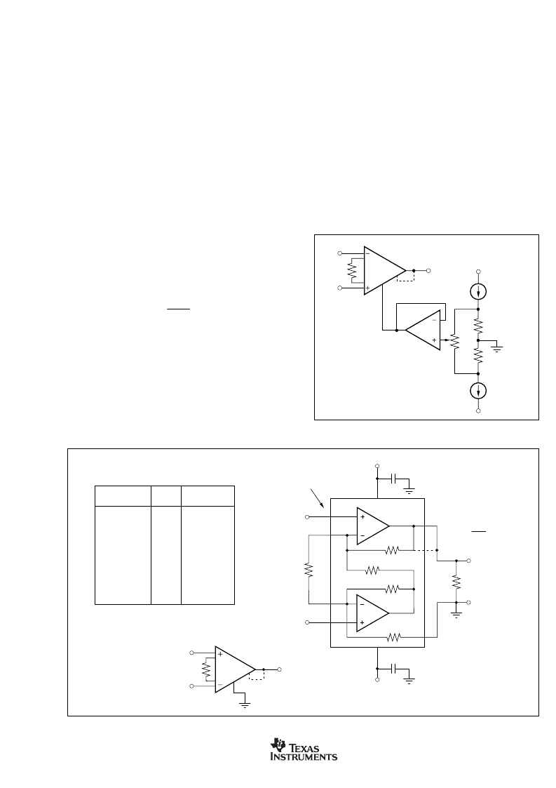
OFFSET TRIMMING
The INA126 and INA2126 are laser trimmed for low offset
voltage and offset voltage drift. Most applications require no
external offset adjustment. Figure 2 shows an optional cir-
cuit for trimming the output offset voltage. The voltage
applied to the Ref terminal is added to the output signal. An
op amp buffer is used to provide low impedance at the Ref
terminal to preserve good common-mode rejection.
FIGURE 1. Basic Connections.
DESIRED GAIN
(V/V)
R
G
(
)
NEAREST 1%
R
G
VALUE
NC
15.8k
5360
1780
845
412
162
80.6
40.2
15.8
7.87
5
10
20
50
100
200
500
1000
2000
5000
10000
NC
16k
5333
1779
842
410
162
80.4
40.1
16.0
8.0
NC: No Connection.
G
= 5+80
k
R
G
FIGURE 2. Optional Trimming of Output Offset Voltage.
10k
OPA237
±10mV
Adjustment Range
100
100
100μA
1/2 REF200
100μA
1/2 REF200
V+
V
–
R
G
INA126
Ref
V
O
V
IN
–
V
IN
+
Dual version has
external sense connection.
40k
10k
10k
40k
INA126
5
4
2
1
8
3
7
6
R
G
R
G
V
IN
A
2
A
1
–
V
IN
+
V
IN
–
V
IN
+
V+
V
–
INA126
0.1
μ
F
0.1
μ
F
V
O
V
O
Ref
Ref
Load
+
–
Also drawn in simplified form:
V
O
= (V
IN
–
V
IN
) G
–
+
G = 5 +
Pin numbers are
for single version
Dual version has
external sense connection.
80k
R
G
相關(guān)PDF資料 |
PDF描述 |
|---|---|
| INA2126UE4 | Micropower single-supply CMOS Instrumentation Amplifier |
| INA2126PAG4 | Micropower single-supply CMOS Instrumentation Amplifier |
| INA2126PG4 | Micropower single-supply CMOS Instrumentation Amplifier |
| INA2128UA | microPower, Single-Supply, CMOS Instrumentation Amplifier |
| INA2128 | microPower, Single-Supply, CMOS Instrumentation Amplifier |
相關(guān)代理商/技術(shù)參數(shù) |
參數(shù)描述 |
|---|---|
| INA2126UE4 | 功能描述:儀表放大器 Micropower Single & Dual Versions RoHS:否 制造商:Texas Instruments 通道數(shù)量: 輸入補償電壓:150 V 可用增益調(diào)整: 最大輸入電阻:10 kOhms 共模抑制比(最小值):88 dB 工作電源電壓:2.7 V to 36 V 電源電流:200 uA 最大工作溫度:+ 125 C 最小工作溫度:- 40 C 封裝 / 箱體:MSOP-8 封裝:Bulk |
| INA2128 | 制造商:BB 制造商全稱:BB 功能描述:Dual, Low Power INSTRUMENTATION AMPLIFIER |
| INA21281K | 制造商:TI 制造商全稱:Texas Instruments 功能描述:Dual, Low Power INSTRUMENTATION AMPLIFIER |
| INA21281KE4 | 制造商:TI 制造商全稱:Texas Instruments 功能描述:Dual, Low Power INSTRUMENTATION AMPLIFIER |
| INA21281KG4 | 制造商:TI 制造商全稱:Texas Instruments 功能描述:Dual, Low Power INSTRUMENTATION AMPLIFIER |
發(fā)布緊急采購,3分鐘左右您將得到回復(fù)。