- 您現(xiàn)在的位置:買賣IC網(wǎng) > PDF目錄383111 > IPP14N03LA (INFINEON TECHNOLOGIES AG) MULTI DVI TRANSMITTER MULTIMODE -FIBER PDF資料下載
參數(shù)資料
| 型號: | IPP14N03LA |
| 廠商: | INFINEON TECHNOLOGIES AG |
| 英文描述: | MULTI DVI TRANSMITTER MULTIMODE -FIBER |
| 中文描述: | 的OptiMOS 2功率晶體管 |
| 文件頁數(shù): | 2/10頁 |
| 文件大小: | 346K |
| 代理商: | IPP14N03LA |
IPB14N03LA
IPI14N03LA, IPP14N03LA
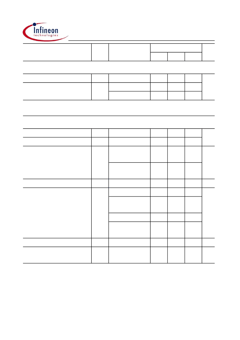
Parameter
Symbol Conditions
Unit
min.
typ.
max.
Thermal characteristics
Thermal resistance, junction - case
R
thJC
-
-
3.2
K/W
SMD version, device on PCB
R
thJA
minimal footprint
-
-
62
6 cm
2
cooling area
4)
-
-
40
Electrical characteristics,
at
T
j
=25 °C, unless otherwise specified
Static characteristics
Drain-source breakdown voltage
V
(BR)DSS
V
GS
=0 V,
I
D
=1 mA
25
-
-
V
Gate threshold voltage
V
GS(th)
V
DS
=
V
GS
,
I
D
=20 μA
1.2
1.6
2
Zero gate voltage drain current
I
DSS
V
DS
=25 V,
V
GS
=0 V,
T
j
=25 °C
-
0.1
1
μA
V
DS
=25 V,
V
GS
=0 V,
T
j
=125 °C
-
10
100
Gate-source leakage current
I
GSS
V
GS
=20 V,
V
DS
=0 V
-
10
100
nA
Drain-source on-state resistance
R
DS(on)
V
GS
=4.5 V,
I
D
=20 A
-
18.5
23.1
m
V
GS
=4.5 V,
I
D
=20 A,
SMD version
-
18.2
22.7
V
GS
=10 V,
I
D
=30 A
-
11.6
13.9
V
GS
=10 V,
I
D
=30 A,
SMD version
-
11.3
13.6
Gate resistance
R
G
-
0.9
-
Transconductance
g
fs
|
V
DS
|>2|
I
D
|
R
DS(on)max
,
I
D
=30 A
17
33
-
S
4)
Device on 40 mm x 40 mm x 1.5 mm epoxy PCB FR4 with 6 cm
2
(one layer, 70 μm thick) copper area for drain
connection. PCB is vertical in still air.
Values
1)
Current is limited by bondwire; with an
R
thJC
=3.2 K/W the chip is able to carry 45 A.
2)
See figure 3
3)
T
j,max
=150 °C and duty cycle
D
<0.25 for
V
GS
<-5 V
Rev. 1.3
page 2
2003-12-18
相關(guān)PDF資料 |
PDF描述 |
|---|---|
| IPB15N03L | OptiMOS Buck converter series |
| IPP15N03L | OptiMOS Buck converter series |
| IPB16CN10NG | OptiMOS㈢2 Power-Transistor |
| IPD16CN10NG | OptiMOS㈢2 Power-Transistor |
| IPI16CN10NG | OptiMOS㈢2 Power-Transistor |
相關(guān)代理商/技術(shù)參數(shù) |
參數(shù)描述 |
|---|---|
| IPP14N03LAXK | 制造商:Infineon Technologies AG 功能描述:Trans MOSFET N-CH 25V 30A 3-Pin(3+Tab) TO-220AB |
| IPP15-1FI | 制造商:Leviton Manufacturing Co 功能描述: |
| IPP15-1FT | 制造商:Leviton Manufacturing Co 功能描述: |
| IPP15-1LA | 制造商:Leviton Manufacturing Co 功能描述: |
| IPP15-1LE | 制造商:Leviton Manufacturing Co 功能描述: |
發(fā)布緊急采購,3分鐘左右您將得到回復。