- 您現(xiàn)在的位置:買賣IC網(wǎng) > PDF目錄377497 > IR21365S (International Rectifier) 3-PHASE BRIDGE DRIVER PDF資料下載
參數(shù)資料
| 型號: | IR21365S |
| 廠商: | International Rectifier |
| 英文描述: | 3-PHASE BRIDGE DRIVER |
| 中文描述: | 3相橋式驅(qū)動器 |
| 文件頁數(shù): | 1/36頁 |
| 文件大小: | 390K |
| 代理商: | IR21365S |
當(dāng)前第1頁第2頁第3頁第4頁第5頁第6頁第7頁第8頁第9頁第10頁第11頁第12頁第13頁第14頁第15頁第16頁第17頁第18頁第19頁第20頁第21頁第22頁第23頁第24頁第25頁第26頁第27頁第28頁第29頁第30頁第31頁第32頁第33頁第34頁第35頁第36頁
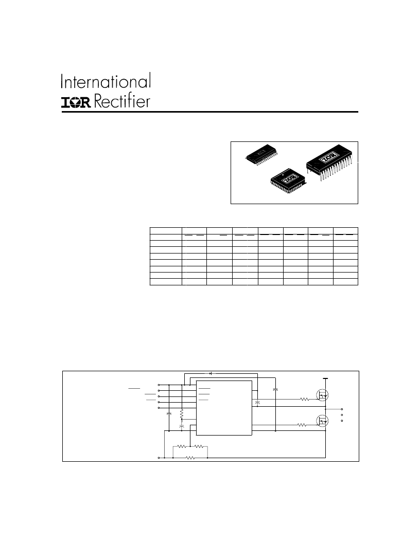
Typical Connection
3-PHASE BRIDGE DRIVER
Packages
Features
Floating channel designed for bootstrap operation
Fully operational to +600V
Tolerant to negative transient voltage - dV/dt immune
Gate drive supply range from 10 to 20V (IR2136/IR21368),
11.5 to 20V (IR21362) or 12 to 20V (IR21363/IR21365/
IR21366/IR21367)
Undervoltage lockout for all channels
Over-current shutdown turns off all six drivers
Independent 3 half-bridge drivers
Matched propagation delay for all channels
Cross-conduction prevention logic
Lowside outputs out of phase with inputs. High side
outputs out of phase (IR2136/IR21363/IR21365/
IR21366/IR21367/IR21368) or in phase
(IR21362) with inputs.
3.3V logic compatible
Lower di/dt gate driver for
better noise immunity
Externally programmable
delay for automatic fault
clear
Also available LEAD-FREE
Data Sheet No. PD60166
revS
IR2136/IR21362/IR21363/IR21365/
IR21366/IR21367/IR21368 (J&S) & (PbF)
www.irf.com
1
(Refer to Lead Assign-
ments for correct pin con-
figuration). This/These
diagram(s) show electri-
cal connections only.
Please refer to our Appli-
cation
Notes
DesignTips for proper cir-
cuit board layout.
and
28-Lead PDIP
28-Lead SOIC
44-Lead PLCC w/o 12 leads
Description
The IR2136/IR21362/IR21363/IR21365/IR21366/IR21367/IR21368(J&S) are high votage, high speed power MOSFET
and IGBT drivers with three independent high and low side referenced output channels for 3-phase applications.
Proprietary HVIC technology enables ruggedized monolithic construction. Logic inputs are compatible with CMOS
or LSTTL outputs, down to 3.3V logic. A current trip function which terminates all six outputs can be derived from
an external current sense resistor. An enable function is available to terminate all six outputs simultaneously. An
open-drain FAULT signal is provided to indicate that an overcurrent or undervoltage shutdown has occurred.
Overcurrent fault conditions are cleared automatically after a delay programmed externally via an RC network
connected to the RCIN input. The output drivers feature a high pulse current buffer stage designed for minimum
driver cross-conduction. Propagation delays are matched to simplify use in high frequency applications. The
floating channel can be used to drive N-channel power MOSFETs or IGBTs in the high side configuration which
operates up to 600 volts.
VCC
HIN1,2,3 / HIN1,2,3
LIN1,2,3
FAULT
ITRIP
RCIN
EN
VSS
COM
LO1,2,3
VS1,2,3
HO1,2,3
VB1,2,3
IR2136(2)(3)(5)(6)(7)(8)
TO
LOAD
VCC
HIN1,2,3 / HIN1,2,3
LIN1,2,3
FAULT
EN
GND
up to 600V
Part
Input Logic
Ton (typ.)
Toff (typ.)
V
IH
(typ.)
V
IL
(typ.)
Vitrip+
UV CC/BS+
UV CC/BS-
IR2136
HIN, LIN
400ns
380ns
2.7V
1.7V
0.46V
8.9V
8.2V
IR21362
HIN/LIN
400ns
380ns
2.7V
1.7V
0.46V
10.4V
9.4V
IR21363
HIN, LIN
400ns
380ns
2.7V
1.7V
0.46V
11.2V
11.0V
IR21365
HIN, LIN
400ns
380ns
2.7V
1.7V
4.3V
11.2V
11.0V
IR21366
HIN, LIN
250ns
180ns
2.0V
1.3V
0.46V
11.2V
11.0V
IR21367
HIN, LIN
250ns
180ns
2.0V
1.3V
4.3V
11.2V
11.0V
IR21368
HIN,LIN
400ns
380ns
2.0V
1.3V
4.3V
8.9V
8.2V
Feature Comparison: IR2136/IR21362/IR21363/
IR21365/IR21366/IR21367/IR21368
相關(guān)PDF資料 |
PDF描述 |
|---|---|
| IR21366J | 3-PHASE BRIDGE DRIVER |
| IR21366PBF | 3-PHASE BRIDGE DRIVER |
| IR21366S | 3-PHASE BRIDGE DRIVER |
| IR21367J | 3-PHASE BRIDGE DRIVER |
| IR21367S | 3-PHASE BRIDGE DRIVER |
相關(guān)代理商/技術(shù)參數(shù) |
參數(shù)描述 |
|---|---|
| IR21365SPbF | 功能描述:功率驅(qū)動器IC 3 PHASE DRVR HI & LO SIDE INPUTS RoHS:否 制造商:Micrel 產(chǎn)品:MOSFET Gate Drivers 類型:Low Cost High or Low Side MOSFET Driver 上升時(shí)間: 下降時(shí)間: 電源電壓-最大:30 V 電源電壓-最小:2.75 V 電源電流: 最大功率耗散: 最大工作溫度:+ 85 C 安裝風(fēng)格:SMD/SMT 封裝 / 箱體:SOIC-8 封裝:Tube |
| IR21365STRPBF | 功能描述:功率驅(qū)動器IC 3Phs Drvr Sft Trn On Invrt 200ns RoHS:否 制造商:Micrel 產(chǎn)品:MOSFET Gate Drivers 類型:Low Cost High or Low Side MOSFET Driver 上升時(shí)間: 下降時(shí)間: 電源電壓-最大:30 V 電源電壓-最小:2.75 V 電源電流: 最大功率耗散: 最大工作溫度:+ 85 C 安裝風(fēng)格:SMD/SMT 封裝 / 箱體:SOIC-8 封裝:Tube |
| IR21366 | 制造商:IRF 制造商全稱:International Rectifier 功能描述:3-PHASE BRIDGE DRIVER |
| IR21366J | 制造商:IRF 制造商全稱:International Rectifier 功能描述:3-PHASE BRIDGE DRIVER |
| IR21366JPBF | 制造商:International Rectifier 功能描述:DRIVER MOSFET 3PH HIGH/LOW 21366 |
發(fā)布緊急采購,3分鐘左右您將得到回復(fù)。