- 您現(xiàn)在的位置:買賣IC網(wǎng) > PDF目錄377521 > IRHM8054 (International Rectifier) HEXFET Transistor(HEXFET 晶體管) PDF資料下載
參數(shù)資料
| 型號: | IRHM8054 |
| 廠商: | International Rectifier |
| 英文描述: | HEXFET Transistor(HEXFET 晶體管) |
| 中文描述: | 的HEXFET晶體管(之HEXFET晶體管) |
| 文件頁數(shù): | 2/8頁 |
| 文件大小: | 129K |
| 代理商: | IRHM8054 |
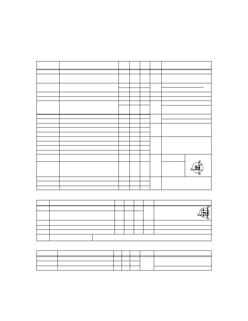
IRHM7054, IRHM8054 Devices
Pre-Irradiation
2
www.irf.com
Electrical Characteristics
@ Tj = 25°C (Unless Otherwise Specified)
Parameter
Drain-to-Source Breakdown Voltage
Temperature Coefficient of Breakdown
Voltage
Static Drain-to-Source
On-State Resistance
Gate Threshold Voltage
Forward Transconductance
Zero Gate Voltage Drain Current
Min
60
—
Typ
—
0.053
Max Units
—
—
Test Conditions
VGS = 0 V, ID = 1.0mA
Reference to 25°C, ID = 1.0mA
BVDSS
BVDSS/
TJ
V
V/°C
RDS(on)
—
—
2.0
12
—
—
—
—
—
—
—
—
0.027
0.030
4.0
—
25
250
VGS = 12V, ID =30A
VGS = 12V, ID = 35A
VDS = VGS, ID = 1.0mA
VDS > 15V, IDS = 30A
VDS= 0.8 x Max Rating,VGS=0V
VDS = 0.8 x Max Rating
VGS = 0V, TJ = 125°C
VGS = 20V
VGS = -20V
VGS = 12V, ID = 35A
VDS = Max Rating x 0.5
V
VGS(th)
gfs
IDSS
S (
)
IGSS
IGSS
Qg
Qgs
Qgd
td
(on)
tr
td
(off)
tf
LD
Gate-to-Source Leakage Forward
Gate-to-Source Leakage Reverse
Total Gate Charge
Gate-to-Source Charge
Gate-to-Drain (‘Miller’) Charge
Turn-On Delay Time
Rise Time
Turn-Off Delay Time
Fall Time
Internal Drain Inductance
—
—
—
—
—
—
—
—
—
—
—
—
—
—
—
—
—
—
—
8.7
100
-100
200
60
75
27
100
75
75
—
nC
VDD = 30V, ID = 35A,
RG = 2.35
LS
Internal Source Inductance
—
8.7
—
Ciss
Coss
Crss
Input Capacitance
Output Capacitance
Reverse Transfer Capacitance
—
—
—
4100
2000
560
—
—
—
VGS = 0V, VDS = 25V
f = 1.0MHz
pF
nA
nH
ns
Measured fromdrain lead,
6mm(0.25 in) frompackage
to center of die.
Measured fromsource lead,
6mm(0.25 in) frompackage
to source bonding pad.
Modified MOSFET symbol show-
μ
A
Source-Drain Diode Ratings and Characteristics
Parameter
IS
Continuous Source Current (Body Diode)
ISM
Pulse Source Current (Body Diode)
Min Typ
—
—
Max Units
35
220
Test Conditions
—
—
Modified MOSFET symbol showing the integral
reverse p-n junction rectifier.
VSD
trr
QRR
ton
Diode Forward Voltage
Reverse Recovery Time
Reverse Recovery Charge
—
—
—
—
—
—
1.4
280
2.2
V
ns
μ
C
T
j
= 25°C, IS = 35A, VGS = 0V
Tj = 25°C, IF = 35A, di/dt
≤
100A/
μ
s
VDD
≤
50V
Forward Turn-On Time
Intrinsic turn-on time is negligible. Turn-on speed is substantially controlled by LS + LD.
A
Thermal Resistance
Parameter
RthJC
Junction-to-Case
RthCS
Junction-to-Sink
RthJA
Junction-to-Ambient
Min Typ Max
—
—
—
0.21
—
—
Units
Test Conditions
0.83
—
48
°C/W
Typical socket mount
* Current is limited by pin diameter.
Rad
相關(guān)PDF資料 |
PDF描述 |
|---|---|
| IRHM7160 | HEXFET Transistor(HEXFET 晶體管) |
| IRHM9130 | P-Channel RAD HARD HEXFET TRANSISTOR(P 溝道 Rad Hard 技術(shù) HEXFET晶體管) |
| IRHM93160 | HEXFET Transistor(HEXFET 晶體管) |
| IRHMS57264SE | RADIATION HARDENED POWER MOSFET THRU-HOLE (Low-Ohmic TO-254AA) 250V, N-CHANNEL |
| IRHMS593160 | RADIATION HARDENED POWER MOSFET THRU-HOLE (Low-Ohmic TO-254AA) |
相關(guān)代理商/技術(shù)參數(shù) |
參數(shù)描述 |
|---|---|
| IRHM8054D | 制造商:未知廠家 制造商全稱:未知廠家 功能描述:TRANSISTOR | MOSFET | N-CHANNEL | 60V V(BR)DSS | 35A I(D) | TO-254VAR |
| IRHM8054U | 制造商:未知廠家 制造商全稱:未知廠家 功能描述:TRANSISTOR | MOSFET | N-CHANNEL | 60V V(BR)DSS | 35A I(D) | TO-254VAR |
| IRHM8064 | 制造商:International Rectifier 功能描述:HEXFET, HIREL, RAD HARD,G4 - Bulk |
| IRHM8130 | 制造商:International Rectifier 功能描述:HIREL, HEXFET RHD - Bulk |
| IRHM8130D | 制造商:未知廠家 制造商全稱:未知廠家 功能描述:TRANSISTOR | MOSFET | N-CHANNEL | 100V V(BR)DSS | 14A I(D) | TO-254VAR |
發(fā)布緊急采購,3分鐘左右您將得到回復(fù)。