- 您現(xiàn)在的位置:買(mǎi)賣(mài)IC網(wǎng) > PDF目錄377521 > IRHN7054 (International Rectifier) HEXFET Transistor(HEXFET 晶體管) PDF資料下載
參數(shù)資料
| 型號(hào): | IRHN7054 |
| 廠商: | International Rectifier |
| 英文描述: | HEXFET Transistor(HEXFET 晶體管) |
| 中文描述: | 的HEXFET晶體管(之HEXFET晶體管) |
| 文件頁(yè)數(shù): | 2/8頁(yè) |
| 文件大小: | 97K |
| 代理商: | IRHN7054 |
IRHN7054, IRHN8054, JANSR-,JANSH-,2N7394U Devices
Pre-Irradiation
2
www.irf.com
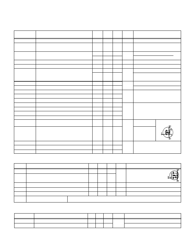
Electrical Characteristics
@ Tj = 25°C (Unless Otherwise Specified)
Parameter
Drain-to-Source Breakdown Voltage
Temperature Coefficient of Breakdown
Voltage
Static Drain-to-Source
On-State Resistance
Gate Threshold Voltage
Forward Transconductance
Zero Gate Voltage Drain Current
Min
60
—
Typ
—
0.053
Max Units
—
—
Test Conditions
VGS = 0 V, ID = 1.0mA
Reference to 25°C, ID = 1.0mA
BVDSS
BVDSS/
TJ
V
V/°C
RDS(on)
—
—
2.0
12
—
—
—
—
—
—
—
—
0.027
0.030
4.0
—
25
250
VGS = 12V, ID =30A
VGS = 12V, ID = 35A
VDS = VGS, ID = 1.0mA
VDS > 15V, IDS = 30A
VDS= 0.8 x Max Rating,VGS=0V
VDS = 0.8 x Max Rating
VGS = 0V, TJ = 125°C
VGS = 20V
VGS = -20V
VGS = 12V, ID = 35A
VDS = Max Rating x 0.5
V
VGS(th)
gfs
IDSS
S (
)
IGSS
IGSS
Qg
Qgs
Qgd
td
(on)
tr
td
(off)
tf
LD
Gate-to-Source Leakage Forward
Gate-to-Source Leakage Reverse
Total Gate Charge
Gate-to-Source Charge
Gate-to-Drain (‘Miller’) Charge
Turn-On Delay Time
Rise Time
Turn-Off Delay Time
Fall Time
Internal Drain Inductance
—
—
—
—
—
—
—
—
—
—
—
—
—
—
—
—
—
—
—
2.0
100
-100
200
60
75
27
100
75
75
—
nC
VDD = 30V, ID = 35A,
RG = 2.35
LS
Internal Source Inductance
—
4.1
—
Ciss
Coss
Crss
Input Capacitance
Output Capacitance
Reverse Transfer Capacitance
—
—
—
4100
2000
560
—
—
—
VGS = 0V, VDS = 25V
f = 1.0MHz
pF
nA
nH
ns
Measured from drain lead,
6mm (0.25 in) from package
to center of die.
Measured from source lead,
6mm (0.25 in) from package
to source bonding pad.
Modified MOSFET symbol show-
ing the internal inductances.
μ
A
Source-Drain Diode Ratings and Characteristics
Parameter
IS
Continuous Source Current (Body Diode)
ISM
Pulse Source Current (Body Diode)
Min Typ
—
—
Max Units
35
283
Test Conditions
—
—
Modified MOSFET symbol showing the integra
rverse p-n junction rectifier.
VSD
trr
QRR
ton
Diode Forward Voltage
Reverse Recovery Time
Reverse Recovery Charge
—
—
—
—
—
—
1.4
280
2.2
V
ns
μ
C
T
j
= 25°C, IS = 35A, VGS = 0V
Tj = 25°C, IF = 35A, di/dt
≤
100A/
μ
s
VDD
≤
50V
Forward Turn-On Time
Intrinsic turn-on time is negligible. Turn-on speed is substantially controlled by LS + LD.
A
.
Thermal Resistance
Parameter
RthJC
Junction-to-Case
RthJ-PCB
Junction-to-PC board
Min Typ Max
—
—
—
6.6
Units
Test Conditions
0.83
— °C/W
相關(guān)PDF資料 |
PDF描述 |
|---|---|
| IRHN8054 | HEXFET Transistor(HEXFET 晶體管) |
| IRHN7130 | TRANSISTOR N-CHANNEL(BVdss=100V, Rds(on)=0.18ohm, Id=14) |
| IRHN8130 | TRANSISTOR N-CHANNEL(BVdss=100V, Rds(on)=0.18ohm, Id=14) |
| IRHN7230 | TRANSISTOR N-CHANNEL(BVdss=200V, Rds(on)=0.40ohm, Id=9.0A) |
| IRHN8230 | TRANSISTOR N-CHANNEL(BVdss=200V, Rds(on)=0.40ohm, Id=9.0A) |
相關(guān)代理商/技術(shù)參數(shù) |
參數(shù)描述 |
|---|---|
| IRHN7130 | 制造商:IRF 制造商全稱(chēng):International Rectifier 功能描述:TRANSISTOR N-CHANNEL(BVdss=100V, Rds(on)=0.18ohm, Id=14) |
| IRHN7150 | 制造商:International Rectifier 功能描述:TRANS MOSFET N-CH 100V 34A 3SMD-1 - Rail/Tube |
| IRHN7230 | 制造商:International Rectifier 功能描述:HIREL, HEXFET RHD - Bulk |
| IRHN7250 | 制造商:International Rectifier 功能描述:HEXFET, HIREL, RAD HARD,G4 - Bulk |
| IRHN7250SE | 制造商:International Rectifier 功能描述:HIREL, HEXFET RHD - Bulk |
發(fā)布緊急采購(gòu),3分鐘左右您將得到回復(fù)。