- 您現在的位置:買賣IC網 > PDF目錄377523 > IRISa6331 (International Rectifier) INTEGRATED SWITCHER PDF資料下載
參數資料
| 型號: | IRISa6331 |
| 廠商: | International Rectifier |
| 英文描述: | INTEGRATED SWITCHER |
| 中文描述: | 多功能開關 |
| 文件頁數: | 2/7頁 |
| 文件大?。?/td> | 379K |
| 代理商: | IRISA6331 |
www.irf.com 2
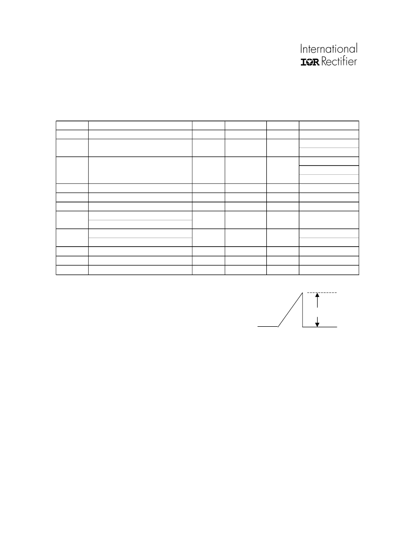
*1 Refer to MOS FET A.S.O curve
*2 MOS FET Tch-EAS curve
*3 Refer to MOS FET Ta-PD1 curve
*4 Refer to TF-PD2 curve for Control IC (See page 5)
*5 Maximum switching current. The maximum switching current is the Drain current determined by the drive
voltage of the IC and threshold voltage (Vth) of MOS FET. Therefore, in the event that voltage drop
occurs between Pin 1and Pin 2 due to patterning, the maximum switching current decreases as shown by
V
1-2
in Fig.1 Accordingly please use this device within the decrease value, referring to the derating
curve of the maximum switching current.
*6 When embedding this hybrid IC onto the printed circuit board (board size 15mm
×
15mm)
Absolute Maximum Ratings (Ta=25
℃
) (Refer Gnd 2 and 5)
Absolute maximum ratings indicate sustained limits beyond which damage to the device may occur. All voltage parameters are
absolute voltages referenced to terminals stated, all currents are defined positive into any lead. The thermal resistance and power
dissipation ratings are measured under board mounted and still air conditions.
IRIS-A6331
Symbol
I
Dpeak
Definition
Terminals Max. Ratings
8
Units
A
Note
Drain Current *1
3.54
Single Pulse
V
1-2
=0.82V
Ta=-20~+125
℃
Single Pulse
V
DD
=99V,L=20mH
I
L
=2.1A
Vin
Vth
P
D1
Input voltage for control part
O.C.P/F.B Pin voltage
Power dissipation for MOSFET *3
Power dissipation for control part
(Control IC) *4
Internal frame temperature
in operation
Operating ambient temperature
Storage temperature
Channel temperature
3-2
4-2
8-1
35
6
1.35
V
V
W
*6
Refer to recommended
operating temperature
Top
Tstg
Tch
-
-
-
-20 ~ +125
-40 ~ +125
150
℃
℃
℃
A
Single pulse avalanche energy *2
8-1
E
AS
32
mJ
Maximum switching current *5
8
I
DMAX
3.54
Specified by
Vin
×
Iin
-
T
F
-20 ~ +125
℃
3-2
P
D2
0.14
W
V
1-2
Fig.1
相關PDF資料 |
PDF描述 |
|---|---|
| IRK.236 | STANDARD RECOVERY DIODES |
| IRKD236-04 | STANDARD RECOVERY DIODES |
| IRK166 | STANDARD RECOVERY DIODES |
| IRK.166 | STANDARD RECOVERY DIODES |
| IRK.196 | STANDARD RECOVERY DIODES |
相關代理商/技術參數 |
參數描述 |
|---|---|
| IRIS-A6331 | 制造商:IRF 制造商全稱:International Rectifier 功能描述:INTEGRATED SWITCHER |
| IRIS-A6351 | 制造商:IRF 制造商全稱:International Rectifier 功能描述:INTEGRATED SWITCHER |
| IRIS-A6359 | 制造商:IRF 制造商全稱:International Rectifier 功能描述:INTEGRATED SWITCHER |
| IRIS-A6372 | 制造商:IRF 制造商全稱:International Rectifier 功能描述:INTEGRATED SWITCHER |
| IRIS-F6426S | 制造商:IRF 制造商全稱:International Rectifier 功能描述:INTEGRATED SWITCHER |
發(fā)布緊急采購,3分鐘左右您將得到回復。