- 您現(xiàn)在的位置:買賣IC網(wǎng) > PDF目錄377538 > IRS2111STRPBF (International Rectifier) HALF-BRIDGE DRIVER PDF資料下載
參數(shù)資料
| 型號: | IRS2111STRPBF |
| 廠商: | International Rectifier |
| 英文描述: | HALF-BRIDGE DRIVER |
| 中文描述: | 半橋驅(qū)動器 |
| 文件頁數(shù): | 2/16頁 |
| 文件大小: | 306K |
| 代理商: | IRS2111STRPBF |
IRS2111(S)PbF
www.irf.com
2
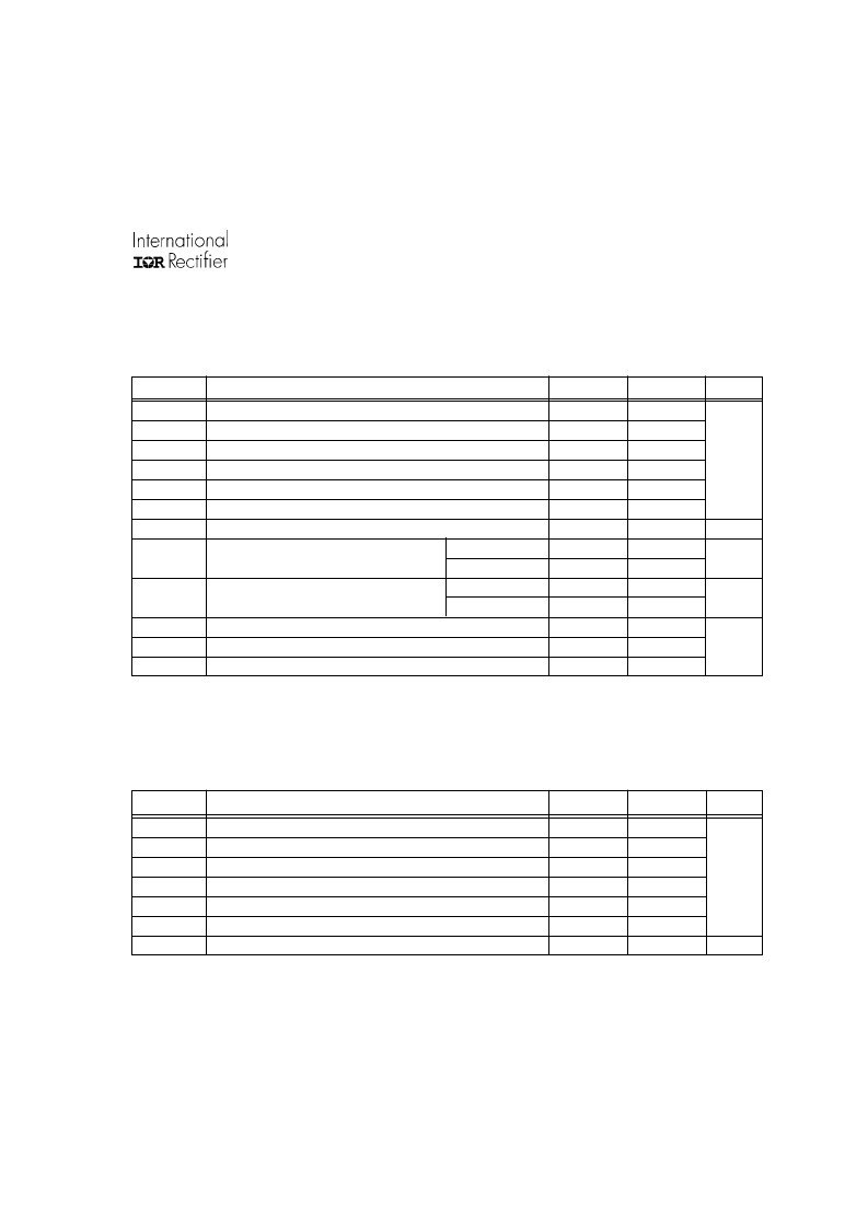
Symbol Definition
V
B
V
S
V
HO
V
CC
V
LO
V
IN
dV
s
/dt
Min.
-0.3
Max.
625 (Note 1)
Units
High side floating supply voltage
High side floating supply offset voltage
V
B
- 25
V
S
- 0.3
-0.3
V
B
+ 0.3
V
B
+ 0.3
25 (Note 1)
High side floating output voltage
Low side and logic fixed supply voltage
Low side output voltage
-0.3
V
CC
+ 0.3
V
CC
+ 0.3
50
Logic input voltage
-0.3
Allowable offset supply voltage transient (Fig. 2)
—
V/ns
P
D
Package power dissipation @ T
≤
+25
°
C (8 Lead PDIP)
(8 lead SOIC)
—
1.0
—
0.625
Rth
JA
Thermal resistance, junction to ambient
(8 lead PDIP)
—
125
(8 lead SOIC)
—
200
T
J
T
S
T
L
Junction temperature
—
150
Storage temperature
-55
150
Lead temperature (soldering, 10 seconds)
—
300
Absolute Maximum Ratings
Absolute maximum ratings indicate sustained limits beyond which damage to the device may occur. All voltage param-
eters are absolute voltages referenced to COM. The thermal resistance and power dissipation ratings are measured
under board mounted and still air conditions. Additional information is shown in Figs. 7 through 10.
V
W
°
C/W
°
C
Symbol Definition
V
B
V
S
V
HO
V
CC
V
LO
V
IN
T
A
Min.
V
S
+ 10
Note 2
Max.
V
S
+ 20
600
Units
High side floating supply absolute voltage
High side floating supply offset voltage
High side floating output voltage
V
S
10
V
B
20
Low side and logic fixed supply voltage
Low side output voltage
0
V
CC
V
CC
125
Logic input voltage
0
Ambient temperature
-40
Note 2: Logic operational for V
S
of -5 V to +600 V. Logic state held for V
S
of -5 V to -V
BS
. (Please refer to the Design Tip
DT97-3 for more details).
Recommended Operating Conditions
The input/output logic timing diagram is shown in Fig. 1. For proper operation the device should be used within the
recommended conditions. The V
S
offset rating is tested with all supplies biased at a 15 V differential.
°
C
V
Note 1: All supplies are fully tested at 25 V, and an internal 20 V clamp exists for each supply
相關(guān)PDF資料 |
PDF描述 |
|---|---|
| IRS2112-1PBF | HIGH AND LOW SIDE DRIVER |
| IRS2112-2PBF | HIGH AND LOW SIDE DRIVER |
| IRS2112PBF | HIGH AND LOW SIDE DRIVER |
| IRS2112SPBF | HIGH AND LOW SIDE DRIVER |
| IRS2112STRPBF | HIGH AND LOW SIDE DRIVER |
相關(guān)代理商/技術(shù)參數(shù) |
參數(shù)描述 |
|---|---|
| IRS2112-1PBF | 制造商:IRF 制造商全稱:International Rectifier 功能描述:HIGH AND LOW SIDE DRIVER |
| IRS2112-2PBF | 制造商:IRF 制造商全稱:International Rectifier 功能描述:HIGH AND LOW SIDE DRIVER |
| IRS2112PBF | 功能描述:功率驅(qū)動器IC Hi&Lw Sd Drvr ShutDwn Inpt RoHS:否 制造商:Micrel 產(chǎn)品:MOSFET Gate Drivers 類型:Low Cost High or Low Side MOSFET Driver 上升時間: 下降時間: 電源電壓-最大:30 V 電源電壓-最小:2.75 V 電源電流: 最大功率耗散: 最大工作溫度:+ 85 C 安裝風格:SMD/SMT 封裝 / 箱體:SOIC-8 封裝:Tube |
| IRS2112PBF | 制造商:International Rectifier 功能描述:MOSFET Driver IC |
| IRS2112SPbF | 功能描述:功率驅(qū)動器IC HI LO SIDE DRVR 600V 200mA 135ns RoHS:否 制造商:Micrel 產(chǎn)品:MOSFET Gate Drivers 類型:Low Cost High or Low Side MOSFET Driver 上升時間: 下降時間: 電源電壓-最大:30 V 電源電壓-最小:2.75 V 電源電流: 最大功率耗散: 最大工作溫度:+ 85 C 安裝風格:SMD/SMT 封裝 / 箱體:SOIC-8 封裝:Tube |
發(fā)布緊急采購,3分鐘左右您將得到回復。