- 您現(xiàn)在的位置:買賣IC網(wǎng) > Datasheet目錄38 > IRS2548DSPBF (International Rectifier)IC PFC Datasheet資料下載
參數(shù)資料
| 型號(hào): | IRS2548DSPBF |
| 廠商: | International Rectifier |
| 文件頁(yè)數(shù): | 13/22頁(yè) |
| 文件大?。?/td> | 320K |
| 描述: | IC PFC |
| 特色產(chǎn)品: | IRS2548D LED Driver |
| 標(biāo)準(zhǔn)包裝: | 55 |
| 系列: | * |
第1頁(yè)第2頁(yè)第3頁(yè)第4頁(yè)第5頁(yè)第6頁(yè)第7頁(yè)第8頁(yè)第9頁(yè)第10頁(yè)第11頁(yè)第12頁(yè)當(dāng)前第13頁(yè)第14頁(yè)第15頁(yè)第16頁(yè)第17頁(yè)第18頁(yè)第19頁(yè)第20頁(yè)第21頁(yè)第22頁(yè)

IRS2548D
www.irf.com
?2011 International Rectifier
13
Application Information and Additional
Details
I. LED Driver Section
Functional Description
Under-voltage Lock-Out Mode (UVLO)
The under-voltage lock-out mode (UVLO) is defined
as the state the IC is in when VCC is below the
turn-on threshold of the IC. The IRS2548D
undervoltage lock-out is designed to maintain an
ultra low supply current and to guarantee the IC is
fully functional before the high and low-side output
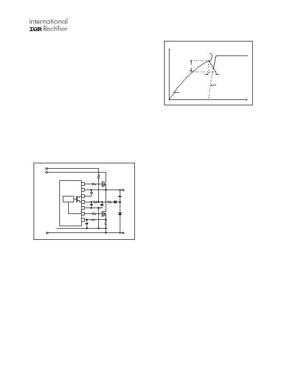
drivers and PFC are activated. Figure 1 shows a
possible VCC supply voltage scheme using the
micro-power start-up current of the IRS2548D
together with a snubber charge pump from the half-
bridge output (R
VCC
, C
VCC1
, C
VCC2
,
C
SNUB
,
D
CP1
and
D
CP2
).
IRS2548D
LO
COM
VB
VS
HO
V
BUS
(+)
V
BUS
(-)
VCC
C
BS
14
MHS
C
VCC2
R
VCC
D
CP1
D
CP2
To Load
R
CS
C
SNUB
MLS
13
12
11
10
9
V
RECT
(+)
C
VCC1
CS
8
R
3
C
CS
IC
COM
Load
Return
R
1
R
2
R
LO
R
HO
BSFET
CONTROL
BSFET
Figure 1: Start-up and supply circuitry.
The VCC capacitors (C
VCC1
and C
VCC2
) are charged
by the current through supply resistor (R
VCC
) minus
the start-up current drawn by the IC. This resistor is
chosen to set the desired AC line input voltage turn-
on threshold for the system. When the voltage at
VCC exceeds the IC start-up threshold (VCCUV+)
and the ENN pin is below 1.5 volts, the IC turns on
and LO begins to oscillate. The capacitors at VCC
begin to discharge due to the increase in IC
operating current (Figure 2). The high-side supply
voltage, VB-VS, begins to increase as capacitor
C
BS
is charged through the internal bootstrap
MOSFET during the LO on-time of each LO
switching cycle. When the VB-VS voltage exceeds
the high-side start-up threshold (VBSUV+), HO
then begins to oscillate. This may take several
cycles of LO to charge VB-VS above VBSUV+ due
to RDSon of the internal bootstrap MOSFET.
DISCHARGE
TIME
INTERNAL VCC
ZENER CLAMP VOLTAGE
VHYST
V
UVLO+
V
UVLO-
CHARGE PUMP
OUTPUT
t
V
C1
R
VCC
& C
VCC1,2
TIME
CONSTANT
C
VCC
DISCHARGE
Figure 2: VCC supply voltage.
When LO and HO are both oscillating, the external
MOSFETs (MHS and MLS) are turned on and off with
a 50% duty cycle and a non-overlapping deadtime of
1.6us. The half-bridge output (pin VS) begins to
switch between the DC bus voltage and COM. During
the deadtime between the turn-off of LO and the turn-
on of HO, the half-bridge output voltage transitions
from COM to the DC bus voltage at a dv/dt rate
determined by the snubber capacitor (C
SNUB
). As the
snubber capacitor charges, current will flow through
the charge pump diode (D
CP2
) to VCC. After several
switching cycles of the half-bridge output, the charge
pump and the internal 15.6V zener clamp of the IC
take over as the supply voltage. Capacitor C
VCC2
supplies the IC current during the VCC discharge
time and should be large enough such that VCC does
not decrease below UVLO- before the charge pump
takes over.
This scheme can be used in non-dimming
applications, however where PWM dimming is used
the charge pump may not supply enough current to
VCC at low dimming levels and in this case an
auxiliary power supply is required.
Capacitor C
VCC1
is required for noise filtering and
must be placed as close as possible and directly
between VCC and COM, and should not be lower
than 0.1uF. Resistors R
1
and R
2
are recommended
for limiting high currents that can flow to VCC from
the charge pump. The internal bootstrap MOSFET
and supply capacitor (C
BS
) provide the floating supply
voltage for the high side driver circuitry. During
UVLO mode the high and low-side driver outputs HO
and LO are both low and the internal oscillator is
disabled.
相關(guān)PDF資料 |
PDF描述 |
|---|---|
| IRS2580DSPBF | IC PFC |
| ISL6111CR-T | IC CTRLR HOT PLUG SWITCH 20-QFN |
| ISL6112INZA-T | IC PWR CNTRLR DUAL SLT 48-TQFP |
| ISL6114IRZA | IC HOT PLUG CTRLR PCI-E 48-QFN |
| 4006-020 | LED CONST CURRENT RESISTOR 20MA |
相關(guān)代理商/技術(shù)參數(shù) |
參數(shù)描述 |
|---|---|
| IRS2548DSPBF | 制造商:International Rectifier 功能描述:IC LED DRVR SOIC |
| IRS2548DSTRPBF | 功能描述:LED照明驅(qū)動(dòng)器 PFC + Hlf Brdg Combo LED Drvr IC RoHS:否 制造商:STMicroelectronics 輸入電壓:11.5 V to 23 V 工作頻率: 最大電源電流:1.7 mA 輸出電流: 最大工作溫度: 安裝風(fēng)格:SMD/SMT 封裝 / 箱體:SO-16N |
| IRS2552D | 制造商:未知廠家 制造商全稱:未知廠家 功能描述:CCFL/EEFL BALLAST CONTROLLER IC |
| IRS2552DPBF | 功能描述:功率驅(qū)動(dòng)器IC CCFL / EEFL Ballast Cntrl IC RoHS:否 制造商:Micrel 產(chǎn)品:MOSFET Gate Drivers 類型:Low Cost High or Low Side MOSFET Driver 上升時(shí)間: 下降時(shí)間: 電源電壓-最大:30 V 電源電壓-最小:2.75 V 電源電流: 最大功率耗散: 最大工作溫度:+ 85 C 安裝風(fēng)格:SMD/SMT 封裝 / 箱體:SOIC-8 封裝:Tube |
| IRS2552DSPBF | 功能描述:功率驅(qū)動(dòng)器IC CCFL / EEFL BALLAST 600V CTRL 300mA RoHS:否 制造商:Micrel 產(chǎn)品:MOSFET Gate Drivers 類型:Low Cost High or Low Side MOSFET Driver 上升時(shí)間: 下降時(shí)間: 電源電壓-最大:30 V 電源電壓-最小:2.75 V 電源電流: 最大功率耗散: 最大工作溫度:+ 85 C 安裝風(fēng)格:SMD/SMT 封裝 / 箱體:SOIC-8 封裝:Tube |
發(fā)布緊急采購(gòu),3分鐘左右您將得到回復(fù)。