- 您現(xiàn)在的位置:買賣IC網(wǎng) > PDF目錄377548 > IS41LV16100-60TL (INTEGRATED SILICON SOLUTION INC) CABLE ASSEMBLY; SMA MALE TO SMA MALE; 93 OHM, RG62A/U COAX; 48" CABLE LENGTH PDF資料下載
參數(shù)資料
| 型號(hào): | IS41LV16100-60TL |
| 廠商: | INTEGRATED SILICON SOLUTION INC |
| 元件分類: | DRAM |
| 英文描述: | CABLE ASSEMBLY; SMA MALE TO SMA MALE; 93 OHM, RG62A/U COAX; 48" CABLE LENGTH |
| 中文描述: | 1M X 16 EDO DRAM, 60 ns, PDSO44 |
| 封裝: | 0.400 INCH, LEADFREE, PLASTIC, TSOP2-50/44 |
| 文件頁數(shù): | 1/20頁 |
| 文件大小: | 123K |
| 代理商: | IS41LV16100-60TL |
IIntegrated Silicon Solution, Inc. — www.issi.com —
1-800-379-4774
Rev. I
04/16/03
1
IS41C16100
IS41LV16100
1M x 16 (16-MBIT) DYNAMIC RAM
WITH EDO PAGE MODE
ISSI
Copyright 2003 Integrated Silicon Solution, Inc. All rights reserved. ISSI reserves the right to make changes to this specification and its products at any time
without notice. ISSI assumes no liability arising out of the application or use of any information, products or services described herein. Customers are advised to
obtain the latest version of this device specification before relying on any published information and before placing orders for products.
FEATURES
TTL compatible inputs and outputs; tristate I/O
Refresh Interval:
— Auto refresh Mode 1,024 cycles /16 ms
—
RAS
-Only,
CAS
-before-
RAS
(CBR), and Hidden
— Self refresh Mode- 1,024 cycles / 128ms
JEDEC standard pinout
Single power supply:
— 5V ± 10% (IS41C16100)
— 3.3V ± 10% (IS41LV16100)
Byte Write and Byte Read operation via two
CAS
Industrail Temperature Range -40
o
C to 85
o
C
DESCRIPTION
The
ISSI
IS41C16100 and IS41LV16100 are 1,048,576 x 16-bit
high-performance CMOS Dynamic Random Access Memories.
These devices offer an accelerated cycle access called EDO Page
Mode. EDO Page Mode allows 1,024 random accesses within a
single row with access cycle time as short as 20 ns per 16-bit word.
The Byte Write control, of upper and lower byte, makes the
IS41C16100 deal for use n 16-bit and 32-bit wide data bus systems.
These features make the IS41C16100and IS41LV16100 deally suited
for high-bandwidth graphics, digital signal processing, high-
performance computing systems, and peripheral applications.
The IS41C16100 and IS41LV16100 are packaged in a 42-pin 400-
mil SOJ and 400-mil 50- (44-) pin TSOP (Type II). The ead-free 400-
mil 50- (44-) option is available too.
KEY TIMING PARAMETERS
Parameter
-50
-60
Unit
Max.
RAS
Access Time (t
RAC
)
50
60
ns
Max.
CAS
Access Time (t
CAC
)
13
15
ns
Max. Column Address Access Time (t
AA
)
25
30
ns
Min. EDO Page Mode Cycle Time (t
PC
)
20
25
ns
Min. Read/Write Cycle Time (t
RC
)
84
104
ns
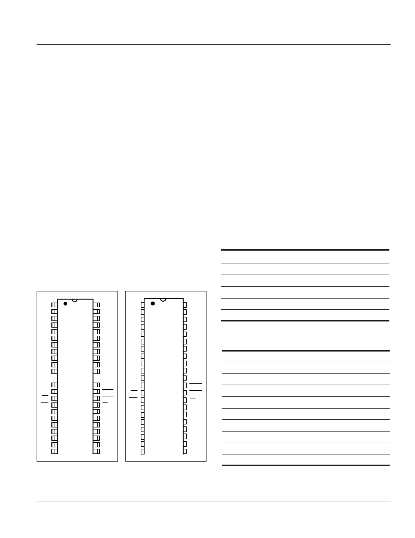
PIN CONFIGURATIONS
50(44)-Pin TSOP (Type II)
42-Pin SOJ
1
2
3
4
5
6
7
8
9
10
11
12
13
14
15
16
17
18
19
20
21
42
41
40
39
38
37
36
35
34
33
32
31
30
29
28
27
26
25
24
23
22
VCC
I/O0
I/O1
I/O2
I/O3
VCC
I/O4
I/O5
I/O6
I/O7
NC
NC
WE
RAS
NC
NC
A0
A1
A2
A3
VCC
GND
I/O15
I/O14
I/O13
I/O12
GND
I/O11
I/O10
I/O9
I/O8
NC
LCAS
UCAS
OE
A9
A8
A7
A6
A5
A4
GND
PIN DESCRIPTIONS
A0-A9
Address Inputs
I/O0-15
Data Inputs/Outputs
WE
Write Enable
OE
Output Enable
RAS
Row Address Strobe
UCAS
Upper Column Address Strobe
LCAS
Lower Column Address Strobe
Vcc
Power
GND
Ground
NC
No Connection
April 2003
1
2
3
4
5
6
7
8
9
10
11
12
13
14
15
16
17
18
19
20
21
22
44
43
42
41
40
39
38
37
36
35
34
33
32
31
30
29
28
27
26
25
24
23
VCC
I/O0
I/O1
I/O2
I/O3
VCC
I/O4
I/O5
I/O6
I/O7
NC
NC
NC
WE
RAS
NC
NC
A0
A1
A2
A3
VCC
GND
I/O15
I/O14
I/O13
I/O12
GND
I/O11
I/O10
I/O9
I/O8
NC
NC
LCAS
UCAS
OE
A9
A8
A7
A6
A5
A4
GND
相關(guān)PDF資料 |
PDF描述 |
|---|---|
| IS41LV16100-60TLI | 1M x 16 (16-MBIT) DYNAMIC RAM WITH EDO PAGE MODE |
| IS41C16128 | 128K x 16 DRAM With EDO Page Mode(128K x 16帶擴(kuò)展數(shù)據(jù)輸出頁模式動(dòng)態(tài)RAM) |
| IS41C4100 | 1Meg x 4 (4-MBIT) DYNAMIC RAM WITH EDO PAGE MODE |
| IS41C4100-35J | 1Meg x 4 (4-MBIT) DYNAMIC RAM WITH EDO PAGE MODE |
| IS41C4100-60J | 1Meg x 4 (4-MBIT) DYNAMIC RAM WITH EDO PAGE MODE |
相關(guān)代理商/技術(shù)參數(shù) |
參數(shù)描述 |
|---|---|
| IS41LV16100-60TLI | 制造商:ISSI 制造商全稱:Integrated Silicon Solution, Inc 功能描述:1M x 16 (16-MBIT) DYNAMIC RAM WITH EDO PAGE MODE |
| IS41LV16100A | 制造商:ISSI 制造商全稱:Integrated Silicon Solution, Inc 功能描述:1M x 16 (16-MBIT) DYNAMIC RAM WITH EDO PAGE MODE |
| IS41LV16100A-50K | 制造商:ISSI 制造商全稱:Integrated Silicon Solution, Inc 功能描述:1M x 16 (16-MBIT) DYNAMIC RAM WITH EDO PAGE MODE |
| IS41LV16100A-50KI | 制造商:ISSI 制造商全稱:Integrated Silicon Solution, Inc 功能描述:1M x 16 (16-MBIT) DYNAMIC RAM WITH EDO PAGE MODE |
| IS41LV16100A-50KL | 制造商:ISSI 制造商全稱:Integrated Silicon Solution, Inc 功能描述:1M x 16 (16-MBIT) DYNAMIC RAM WITH EDO PAGE MODE |
發(fā)布緊急采購(gòu),3分鐘左右您將得到回復(fù)。