- 您現(xiàn)在的位置:買賣IC網(wǎng) > PDF目錄377578 > IS93C46D-2ZLI (INTEGRATED SILICON SOLUTION INC) 1-KBIT SERIAL ELECTRICALLY ERASABLE PROM PDF資料下載
參數(shù)資料
| 型號(hào): | IS93C46D-2ZLI |
| 廠商: | INTEGRATED SILICON SOLUTION INC |
| 元件分類: | DRAM |
| 英文描述: | 1-KBIT SERIAL ELECTRICALLY ERASABLE PROM |
| 中文描述: | 64 X 16 MICROWIRE BUS SERIAL EEPROM, PDSO8 |
| 封裝: | 0.169 INCH, LEAD FREE, MO-153, TSSOP-8 |
| 文件頁數(shù): | 1/15頁 |
| 文件大小: | 130K |
| 代理商: | IS93C46D-2ZLI |
Integrated Silicon Solution, Inc. — www.issi.com —
1-800-379-4774
Rev. 00E
10/25/05
1
IS93C46D
ISSI
Copyright 2005 Integrated Silicon Solution, Inc. All rights reserved. ISSI reserves the right to make changes to this specification and its products at any time
without notice. ISSI assumes no liability arising out of the application or use of any information, products or services described herein. Customers are advised to
obtain the latest version of this device specification before relying on any published information and before placing orders for products.
1-KBIT SERIAL ELECTRICALLY
ERASABLE PROM
ADVANCED INFORMATION
NOVEMBER 2005
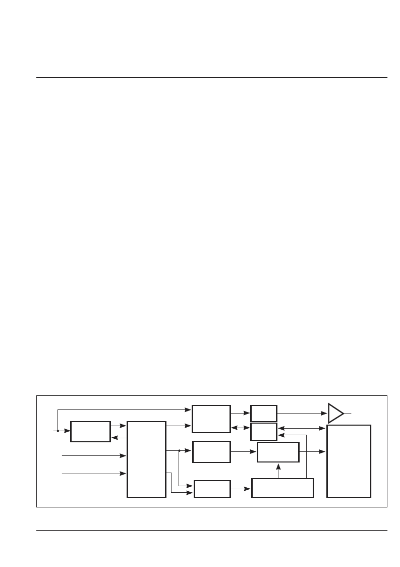
FUNCTIONAL BLOCK DIAGRAM
CS
SK
D
IN
D
OUT
DUMMY
BIT
R/W
AMPS
DATA
REGISTER
ADDRESS
REGISTER
ADDRESS
DECODER
WRITE
ENABLE
HIGH VOLTAGE
GENERATOR
INSTRUCTION
DECODE,
CONTROL,
AND
CLOCK
GENERATION
EEPROM
ARRAY
128x8
64x16
INSTRUCTION
REGISTER
FEATURES
Industry-standard Microwire Interface
— Non-volatile data storage
— Wide voltage operation:
Vcc = 1.8V to 5.5V
— Full TTL compatible inputs and outputs
— Auto increment for efficient data dump
User Configured Memory Organization
— By 16-bit or by 8-bit
Hardware and software write protection
— Defaults to write-disabled state at power-up
— Software instructions for write-enable/disable
Enhanced low voltage CMOS E
2
PROM
technology
Versatile, easy-to-use Interface
— Self-timed programming cycle
— Automatic erase-before-write
— Programming status indicator
— Word and chip erasable
— Chip select enables power savings
Durable and reliable
— 40-year data retention after 1M write cycles
— 1 million write cycles
— Unlimited read cycles
— Schmitt-trigger inputs
Lead-free available
DESCRIPTION
The IS93C46D is a 1Kb non-volatile, ISSI
serial
EEPROM. It is fabricated using an enhanced
CMOS design and process. The IS93C46D
contains power-efficient read/write memory, and
organization of 128 bytes of 8 bits or 64 words of
16 bits. When the ORG pin is connected to Vcc
or left unconnected, x16 is selected; when it is
connected to ground, x8 is selected.
An instruction set defines the operation of the
devices, including read, write, and mode-enable
functions. To protect against inadvertent data
modification, all erase and write instructions are
accepted only while the device is write-enabled. A
selected x8 byte or x16 word can be modified with
a single WRITE or ERASE instruction.
Additionally, the two instructions WRITE ALL or
ERASE ALL can program the entire array. Once
a device begins its self-timed program procedure,
the data out pin (Dout) can indicate the READY/
BUSY
status by raising chip select (CS). The self-
timed write cycle includes an automatic erase-
before-write capability. The device can output any
number of consecutive bytes/words using a single
READ instruction.
相關(guān)PDF資料 |
PDF描述 |
|---|---|
| IS93C56-3G | 2,048-BIT SERIAL ELECTRICALLY ERASABLE PROM |
| IS93C56-3GI | 2,048-BIT SERIAL ELECTRICALLY ERASABLE PROM |
| IS93C56-3GR | 2,048-BIT SERIAL ELECTRICALLY ERASABLE PROM |
| IS93C56-3GRI | 2,048-BIT SERIAL ELECTRICALLY ERASABLE PROM |
| IS93C56-3P | 2,048-BIT SERIAL ELECTRICALLY ERASABLE PROM |
相關(guān)代理商/技術(shù)參數(shù) |
參數(shù)描述 |
|---|---|
| IS93C46D-2ZLI-TR | 功能描述:電可擦除可編程只讀存儲(chǔ)器 1.8V 1Kb Industrial Temp RoHS:否 制造商:Atmel 存儲(chǔ)容量:2 Kbit 組織:256 B x 8 數(shù)據(jù)保留:100 yr 最大時(shí)鐘頻率:1000 KHz 最大工作電流:6 uA 工作電源電壓:1.7 V to 5.5 V 最大工作溫度:+ 85 C 安裝風(fēng)格:SMD/SMT 封裝 / 箱體:SOIC-8 |
| IS93C46D-3GRLA3 | 制造商:ISSI 制造商全稱:Integrated Silicon Solution, Inc 功能描述:1-KBIT SERIAL ELECTRICALLY ERASABLE PROM |
| IS93C46D-3PLA3 | 制造商:ISSI 制造商全稱:Integrated Silicon Solution, Inc 功能描述:1-KBIT SERIAL ELECTRICALLY ERASABLE PROM |
| IS93C56 | 制造商:未知廠家 制造商全稱:未知廠家 功能描述: |
| IS93C56-3 | 制造商:ISSI 制造商全稱:Integrated Silicon Solution, Inc 功能描述:2,048-BIT SERIAL ELECTRICALLY ERASABLE PROM |
發(fā)布緊急采購,3分鐘左右您將得到回復(fù)。