- 您現(xiàn)在的位置:買賣IC網(wǎng) > PDF目錄383135 > ISL55291IUZ-T13 (INTERSIL CORP) Single and Dual Ultra-Low Noise, Ultra-Low Distortion, Rail-to-Rail, Low Power Op Amp PDF資料下載
參數(shù)資料
| 型號(hào): | ISL55291IUZ-T13 |
| 廠商: | INTERSIL CORP |
| 元件分類: | 運(yùn)動(dòng)控制電子 |
| 英文描述: | Single and Dual Ultra-Low Noise, Ultra-Low Distortion, Rail-to-Rail, Low Power Op Amp |
| 中文描述: | DUAL OP-AMP, 800 uV OFFSET-MAX, 800 MHz BAND WIDTH, PDSO10 |
| 封裝: | ROHS COMPLIANT, MSOP-10 |
| 文件頁數(shù): | 4/18頁 |
| 文件大?。?/td> | 886K |
| 代理商: | ISL55291IUZ-T13 |
4
FN6263.1
March 30, 2007
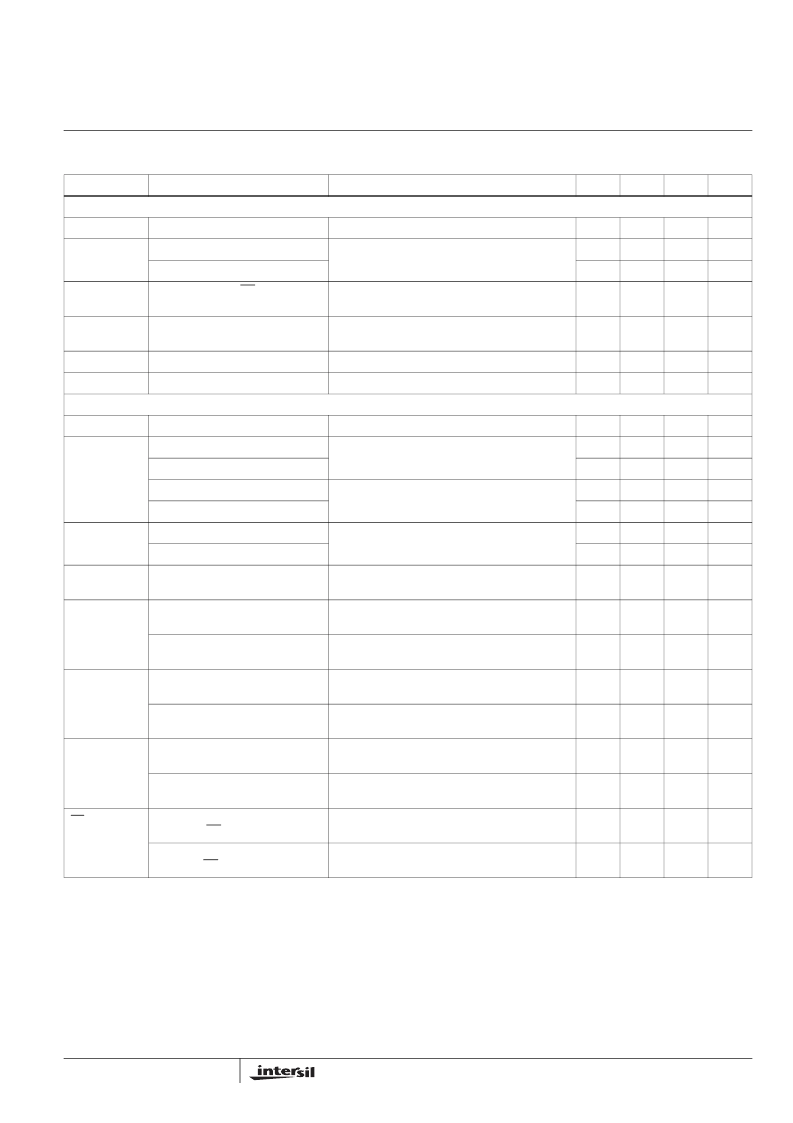
AC SPECIFICATIONS
GBW
Gain Bandwidth Product
A
V
= +10; V
OUT
= 100mV
P-P
; R
f
/R
g
= 909
Ω/
100
Ω
800
MHz
HD
(4MHz)
2nd Harmonic Distortion
A
V
= +10; V
OUT
= 2V
P-P
; R
f
/R
g
= 909
Ω/
100
Ω
-94
dBc
3rd Harmonic Distortion
-104
dBc
ISO
Off-state Isolation; EN = 1 ISL55291;
EN = 0 ISL55191
f
O
= 10MHz; A
V
= +10; V
IN
= 640mV
P-P
;
R
f
/R
g
= 909
Ω/
100
Ω;
C
L
= 1.2pF
-65
dB
X-TALK
ISL55291
Channel to Channel Crosstalk
f
O
= 10MHz; A
V
= +10; V
OUT
(Driven Channel) =
640mV
P-P
; R
f
/R
g
= 909
Ω/
100
Ω;
C
L
= 1.2pF
-75
dB
V
N
Input Referred Voltage Noise
f
O
= 1kHz
1.2
nV/
√
Hz
IN
Input Referred Current Noise
f
O
= 10kHz
3.8
pA/
√
Hz
TRANSIENT RESPONSE
SR
Slew Rate
150
260
V/uS
t
r
, t
f
Large
Signal
Rise Time, t
r
10% to 90%
A
V
= +10; V
OUT
= 3.5V
P-P
; R
f
/R
g
= 909
Ω
/100
Ω
C
L
= 1.2pF
6.6
ns
Fall Time, t
f
10% to 90%
5.7
ns
Rise Time, t
r
10% to 90%
A
V
= +10; V
OUT
= 1V
P-P
; R
f
/R
g
= 909
Ω/
100
Ω
C
L
= 1.2pF
5
ns
Fall Time, t
f
10% to 90%
4
ns
t
r
, t
f
, Small
Signal
Rise Time, t
r
10% to 90%
A
V
= +10; V
OUT
= 100mV
P-P
; R
f
/R
g
= 909
Ω/
100
Ω
C
L
= 1.2pF
3
ns
Fall Time, t
f
10% to 90%
3
ns
t
pd
Propagation Delay
10% V
IN
to 10% V
OUT
A
V
= +10; V
OUT
= 100mV
P-P
; R
f
/R
g
= 909
Ω/
100
Ω
C
L
= 1.2pF
1.6
ns
t
IOL
Positive Input Overload Recovery
Time, t
IOL+
; 10% V
IN
to 10% V
OUT
V
S
= ±2.5V; A
V
= +10; V
IN
= +V
CM
+0.5V;
R
f
/R
g
= 909
Ω/
100
Ω;
C
L
= 1.2pF
50
ns
Negative Input Overload Recovery
Time, t
IOL-
; 10% V
IN
to 10% V
OUT
V
S
= ±2.5V; A
V
= +10; V
IN
= -V -0.5V;
R
f
/R
g
= 909
Ω/
100
Ω;
C
L
= 1.2pF
30
ns
t
OOL
Positive Output Overload Recovery
Time, t
OOL+
; 10% V
IN
to 10% V
OUT
V
S
= ±2.5V; A
V
= +10; V
IN
= 2.3V
P-P
;
R
f
/R
g
= 909
Ω/
100
Ω;
C
L
= 1.2pF
40
ns
Negative Output Overload Recovery
Time, t
OOL-
; 10% V
IN
to 10% V
OUT
V
S
= ±2.5V; A
V
= +10; V
IN
= 2.3V
P-P
;
R
f
/R
g
= 909
Ω/
100
Ω;
C
L
= 1.2pF
30
ns
t
EN
ISL55191
ENABLE to Output Turn-on Delay
Time; 10% EN to 10% V
OUT
A
V
= +10; V
IN
= 500mV
P-P
; R
f
/R
g
= 909
Ω/
100
Ω
C
L
= 1.2pF
540
ns
ENABLE to Output Turn-off Delay
Time; 10% EN to 10% V
OUT
A
V
= +10; V
IN
= 500mV
P-P
; R
f
/R
g
= 909
Ω/
100
Ω
C
L
= 1.2pF
390
ns
t
EN
ISL55291
ENABLE to Output Turn-on Delay
Time; 10% EN to 10% V
OUT
A
V
= +10; V
IN
= 500mV
P-P
; R
f
/R
g
= 909
Ω/
100
Ω
C
L
= 1.2pF
330
ns
ENABLE to Output Turn-off Delay
Time;10% EN to 10% V
OUT
A
V
= +10; V
IN
= 500mV
P-P
; R
f
/R
g
= 909
Ω/
100
Ω
C
L
= 1.2pF
50
ns
Electrical Specifications
V
+
= 5V, V- = GND, R
L
= 1k
Ω,
R
G
= 30
Ω,
R
F
= 270
Ω.
unless otherwise specified. Parameters are per amplifier.
All values are at V+ = 5V, T
A
= +25°C.
PARAMETER
DESCRIPTION
CONDITIONS
MIN
TYP
MAX
UNIT
ISL55191, ISL55291
相關(guān)PDF資料 |
PDF描述 |
|---|---|
| ISL5571AIBZ | Access High Voltage Switch |
| ISL5571A | Access High Voltage Switch |
| ISL5571AIB | Access High Voltage Switch |
| ISL5585 | 3.3V Ringing SLIC Family for Voice Over Broadband VOB |
| ISL5585BIM | 3.3V Ringing SLIC Family for Voice Over Broadband VOB |
相關(guān)代理商/技術(shù)參數(shù) |
參數(shù)描述 |
|---|---|
| ISL5571A | 制造商:INTERSIL 制造商全稱:Intersil Corporation 功能描述:Access High Voltage Switch |
| ISL5571A/B-EVAL1 | 制造商:Intersil Corporation 功能描述:EVALUATION BOARD FOR ISL5571 LINE CARD ACCESS SWITCH - Bulk |
| ISL5571A_04 | 制造商:INTERSIL 制造商全稱:Intersil Corporation 功能描述:Access High Voltage Switch |
| ISL5571AIB | 制造商:Rochester Electronics LLC 功能描述: 制造商:Intersil Corporation 功能描述: |
| ISL5571AIBS2682 | 制造商:Rochester Electronics LLC 功能描述:- Bulk |
發(fā)布緊急采購,3分鐘左右您將得到回復(fù)。
