- 您現(xiàn)在的位置:買賣IC網 > PDF目錄383135 > ISL5571AIBZ (INTERSIL CORP) Access High Voltage Switch PDF資料下載
參數資料
| 型號: | ISL5571AIBZ |
| 廠商: | INTERSIL CORP |
| 元件分類: | 通信及網絡 |
| 英文描述: | Access High Voltage Switch |
| 中文描述: | SPECIALTY TELECOM CIRCUIT, PDSO16 |
| 封裝: | LEAD FREE, PLASTIC, MS-013AA, SOIC-16 |
| 文件頁數: | 3/12頁 |
| 文件大小: | 190K |
| 代理商: | ISL5571AIBZ |
3
Electrical Specifications
T
A
= -40°C to 85°C, Unless Otherwise Specified
Absolute Maximum Ratings
T
A
= 25
°
C
Maximum Supply Voltages
(V
DD
) . . . . . . . . . . . . . . . . . . . . . . . . . . . . . . . . . . . . .-0.5V to +7V
(V
BAT
) . . . . . . . . . . . . . . . . . . . . . . . . . . . . . . . . . . .-19V to -100V
ESD Rating (Human Body Model). . . . . . . . . . . . . . . . . . . . . . .500V
Thermal Information
Die Characteristics
Substrate Potential. . . . . . . . . . . . . . . . . . . . . . . . . . . . . . . . . . V
BAT
Process . . . . . . . . . . . . . . . . . . . . . . . .6-inch BIMOS Bonded Wafer
Thermal Resistance (Typical, Note 1)
SOIC . . . . . . . . . . . . . . . . . . . . . . . . . . . . . . . . . . . .
Maximum Junction Temperature Plastic . . . . . . . . . . . . . . . . .150
°
C
Maximum Storage Temperature Range . . . . . . . . . -65
°
C to 150
°
C
Maximum Lead Temperature (Soldering 10s). . . . . . . . . . . . .300
°
C
(SOIC - Lead Tips Only)
θ
JA
(
°
C/W)
100
CAUTION: Stresses above those listed in “Absolute Maximum Ratings” may cause permanent damage to the device. This is a stress only rating and operation of the
device at these or any other conditions above those indicated in the operational sections of this specification is not implied.
NOTE:
1.
θ
JA
is measured with the component mounted on a low effective thermal conductivity test board in free air. See Tech Brief TB379 for details.
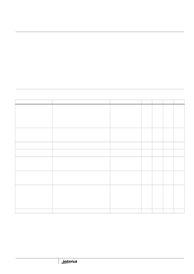
TABLE 1. BREAK SWITCHES - ISL5571A - SW1, SW2
PARAMETER
TEST CONDITION
MEASURE
MIN
TYP
MAX
UNITS
OFF-State Leakage Current:
-40°C
25°C
85°C
V
SWITCH (DIFFERENTIAL)
= -310V to GND
V
SWITCH (DIFFERENTIAL)
= -60V to +250V
V
SWITCH (DIFFERENTIAL)
= -320V to GND
V
SWITCH (DIFFERENTIAL)
= -60V to +260V
V
SWITCH (DIFFERENTIAL)
= -330V to GND
V
SWITCH (DIFFERENTIAL)
= -60V to +270V
I
SWITCH
I
SWITCH
I
SWITCH
-
-
-
-
-
-
1
1
1
μ
A
μ
A
μ
A
ON-Resistance:
-40°C
25°C
85°C
T
LINE
=
±
10mA,
±
40mA, T
BAT
= -2V
T
LINE
=
±
10mA,
±
40mA, T
BAT
= -2V
T
LINE
=
±
10mA,
±
40mA, T
BAT
= -2V
Per ON-resistance Test Condition of SW1, SW2
V
ON
V
ON
V
ON
Magnitude
r
ON
SW1 - r
ON
SW2
V
ON
-
-
-
12
16
-
0.05
-
-
28
0.5
ON-Resistance Match
ON-State Voltage (Note 2)
Break Switches in ON-State; I
switch
= I
LIMIT
at
50/60Hz
-
-
220
V
Peak
DC Current Limit:
-40°C
25°C
85°C
V
SWITCH (ON)
=
±
10V
V
SWITCH (ON)
=
±
10V
V
SWITCH (ON)
=
±
10V
Break Switches in ON-state; Ringing Access
Switches OFF; Apply
±
1000V at 10/1000
μ
s
Pulse; Appropriate External Secondary
Protection in Place
I
SWITCH
I
SWITCH
I
SWITCH
I
SWITCH
-
-
80
-
-
125
-
1.5
250
-
mA
mA
mA
A
Dynamic Current Limit
(t = <0.5
μ
s)
2.0
Isolation:
-40°C
25°C
85°C
V
SWITCH
(Both Poles) =
±
310V
Logic Inputs = GND
V
SWITCH
(Both Poles) =
±
320V
Logic Inputs = GND
V
SWITCH
(Both Poles) =
±
330V
Logic Inputs = GND
I
SWITCH
I
SWITCH
I
SWITCH
-
-
-
-
-
-
1
1
1
μ
A
μ
A
μ
A
dV/dt Sensitivity (Note 3)
NOTES:
2. Choice of secondary protection should ensure this rating is not exceeded.
3. Applied voltage is 100V
P-P
square wave at 100Hz.
-
5000
-
V/
μ
s
ISL5571A
相關PDF資料 |
PDF描述 |
|---|---|
| ISL5571A | Access High Voltage Switch |
| ISL5571AIB | Access High Voltage Switch |
| ISL5585 | 3.3V Ringing SLIC Family for Voice Over Broadband VOB |
| ISL5585BIM | 3.3V Ringing SLIC Family for Voice Over Broadband VOB |
| ISL5585CIM | 3.3V Ringing SLIC Family for Voice Over Broadband VOB |
相關代理商/技術參數 |
參數描述 |
|---|---|
| ISL5571AIBZS2693 | 制造商:Intersil Corporation 功能描述:PB-FREE SUBSCRIBER LINE ACCESS SWITCH - Rail/Tube |
| ISL5571AIBZ-T | 功能描述:模擬開關 IC Pb-Free SUBSCRIBER LINE ACCESS SWITCH IN TAPE & REEL RoHS:否 制造商:Texas Instruments 開關數量:2 開關配置:SPDT 開啟電阻(最大值):0.1 Ohms 切換電壓(最大): 開啟時間(最大值): 關閉時間(最大值): 工作電源電壓:2.7 V to 4.5 V 最大工作溫度:+ 85 C 安裝風格:SMD/SMT 封裝 / 箱體:DSBGA-16 |
| ISL5571AIBZ-TS2693 | 制造商:Intersil Corporation 功能描述:PB-FREE SUBSCRIBER LINE ACCESS SWITCH IN TAPE & REEL - Tape and Reel |
| ISL5585 | 制造商:INTERSIL 制造商全稱:Intersil Corporation 功能描述:3.3V Ringing SLIC Family for Voice Over Broadband VOB |
| ISL5585_04 | 制造商:INTERSIL 制造商全稱:Intersil Corporation 功能描述:3.3V Ringing SLIC Family for Voice Over Broadband (VOB) |
發(fā)布緊急采購,3分鐘左右您將得到回復。