- 您現(xiàn)在的位置:買(mǎi)賣(mài)IC網(wǎng) > PDF目錄383143 > ISL6225CAZ-T (INTERSIL CORP) KJ SERIES II PDF資料下載
參數(shù)資料
| 型號(hào): | ISL6225CAZ-T |
| 廠商: | INTERSIL CORP |
| 元件分類: | 穩(wěn)壓器 |
| 英文描述: | KJ SERIES II |
| 中文描述: | DUAL SWITCHING CONTROLLER, 345 kHz SWITCHING FREQ-MAX, PDSO28 |
| 封裝: | PLASTIC, LEAD FREE, SSOP-28 |
| 文件頁(yè)數(shù): | 13/19頁(yè) |
| 文件大小: | 522K |
| 代理商: | ISL6225CAZ-T |
第1頁(yè)第2頁(yè)第3頁(yè)第4頁(yè)第5頁(yè)第6頁(yè)第7頁(yè)第8頁(yè)第9頁(yè)第10頁(yè)第11頁(yè)第12頁(yè)當(dāng)前第13頁(yè)第14頁(yè)第15頁(yè)第16頁(yè)第17頁(yè)第18頁(yè)第19頁(yè)
13
FN9049.7
December 28, 2004
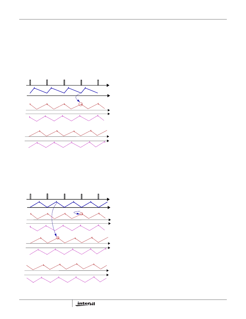
This makes out-of-phase channel synchronization
undesirable when one of the channels is running on a duty-
factor of 50%. Inversely, the in-phase channel arrangement
does not have this drawback. Points of decision are far from
noisy moments of time in both sourcing and sinking modes
of operation for V
IN
= 7.5V to 24V as it is shown in Figure 9.
In the case when power for VDDQ is taken from the +5V
system rail, as Figure 10 shows, both in-phase and out-of-
phase approaches are susceptible to noise in the sourcing
mode.
Noise immunity can be improved by operating the VTT
converter with a 90
o
phase shift. As the time diagrams in
Figure 10 show, the points of concern are always about a
quarter of the period away from the noise emitting
transitions.
Several ways of synchronization are implemented into the
chip. When the DDR pin is connected to GND, the channels
operate 180
o
out-of-phase. In the DDR mode when the DDR
pin is connected to V
CC
, the channels operate either in-
phase when the V
IN
pin is connected to the input voltage
source, or with 90
o
phase shift if the VIN pin is connected to
GND.
ISL6225 DC-DC Converter Application
Circuits
Figures 11 and 12 show application circuits of a dual channel
DC/DC converter for a notebook PC.
The power supply in Figure 11 provides +2.5V and +1.8V for
memory and graphic interface chipset from +5.0V to +24V
battery voltage.
Figure 12 shows the power supply that provides +2.5V and
+1.8V for memory and graphic interface chipset from +5.0V
system rail.
Figure 13 shows an application circuit for a single-output
split input power supply with current sharing for advanced
graphic card applications.
Figure 14 and 15 show application circuits of a complete
power solution for DDR memory that becomes a preferred
choice in modern computers. The power supply shown in
Figure 14 generates +2.5V VDDQ voltage from +5.0V to
+24V battery voltage. The +1.25V VTT termination voltage
tracks VDDQ/2 and is derived from +2.5V VDDQ. To
complete the DDR memory power requirements, the +1.25V
reference voltage is also provided. The PG2 pin serves as
an output for the reference voltage in this mode.
Figure 15 depicts the DDR solution in the case where the 5V
system rail is used as a primary voltage source.
For detailed information on the circuit, including a Bill-of-
Materials and circuit board description, see Application Note
AN9995. Also see Intersil’s web site (http://www.intersil.com)
for the latest information.
FIGURE 9. CHANNEL INTERFERENCE V
IN
= 7.5V...24V
OUT-OF-PHASE
IN-PHASE
SOURCING
SINKING
SINKING
SOURCING
VTT
VTT
300kHz CLOCK
VDDQ
FIGURE 10. CHANNEL INTERFERENCE V
IN
= 5V
OUT-OF-PHASE
IN-PHASE
SOURCING
SINKING
SINKING
SOURCING
300kHz CLOCK
VTT
VTT
VDDQ
90
o
PHASE SHIFT
SINKING
SOURCING
VTT
ISL6225
相關(guān)PDF資料 |
PDF描述 |
|---|---|
| ISL6225 | Dual Mobile-Friendly PWM Controller with DDR Memory Option(帶DDR存儲(chǔ)器選項(xiàng)的雙移動(dòng)型PWM控制器) |
| ISL6225CA | Octal D-Type Transparent Latches With 3-State Outputs 20-SSOP -40 to 85 |
| ISL6225CA-T | Dual Mobile-Friendly PWM Controller with DDR Memory Option |
| ISL6225CAZA | Dual Mobile-Friendly PWM Controller with DDR Memory Option |
| ISL6226 | Advanced PWM and Linear Power Controller for Portable Applications |
相關(guān)代理商/技術(shù)參數(shù) |
參數(shù)描述 |
|---|---|
| ISL6226 | 制造商:INTERSIL 制造商全稱:Intersil Corporation 功能描述:Advanced PWM and Linear Power Controller for Portable Applications |
| ISL6226CA | 制造商:Rochester Electronics LLC 功能描述:- Bulk 制造商:Intersil Corporation 功能描述: |
| ISL6226EVAL1 | 制造商:INTERSIL 制造商全稱:Intersil Corporation 功能描述:Advanced PWM and Linear Power Controller for Portable Applications |
| ISL6227 | 制造商:INTERSIL 制造商全稱:Intersil Corporation 功能描述:Dual Mobile-Friendly PWM Controller with DDR Option |
| ISL6227_07 | 制造商:INTERSIL 制造商全稱:Intersil Corporation 功能描述:Dual Mobile-Friendly PWM Controller with DDR Option |
發(fā)布緊急采購(gòu),3分鐘左右您將得到回復(fù)。