- 您現(xiàn)在的位置:買賣IC網(wǎng) > PDF目錄383143 > ISL6244HR-T (INTERSIL CORP) Test Probe; Range:-32deg to 500degF RoHS Compliant: NA PDF資料下載
參數(shù)資料
| 型號: | ISL6244HR-T |
| 廠商: | INTERSIL CORP |
| 元件分類: | 穩(wěn)壓器 |
| 英文描述: | Test Probe; Range:-32deg to 500degF RoHS Compliant: NA |
| 中文描述: | SWITCHING CONTROLLER, 1000 kHz SWITCHING FREQ-MAX, PQCC32 |
| 封裝: | 5 X 5 MM, PLASTIC, MO-220-VHHD, QFN-32 |
| 文件頁數(shù): | 3/25頁 |
| 文件大?。?/td> | 845K |
| 代理商: | ISL6244HR-T |
3
FN9106.3
December 28, 2004
Absolute Maximum Ratings
Supply Voltage, VCC (Note 3) . . . . . . . . . . . . . . . . . . . . . . . . . . .+7V
Input, Output, or I/O Voltage . . . . . . . . . . GND -0.3V to V
CC
+ 0.3V
ESD Classification . . . . . . . . . . . . . . . . . . . . . . . . . . . . . . . . .Class II
Operating Conditions
Supply Voltage, VCC . . . . . . . . . . . . . . . . . . . . . . . . . . . . . +5V ±5%
Ambient Temperature. . . . . . . . . . . . . . . . . . . . . . . . .-10°C to 100°C
Maximum Junction Temperature . . . . . . . . . . . . . . . . . . . . . . .125°C
Thermal Information
Thermal Resistance
QFN Package (Notes 4, 6). . . . . . . . . .
Maximum Junction Temperature . . . . . . . . . . . . . . . . . . . . . . . 150°C
Maximum Storage Temperature Range. . . . . . . . . . .-65°C to 150°C
Maximum Lead Temperature (Soldering 10s) . . . . . . . . . . . . . 300°C
θ
JA
(°C/W)
32
θ
JC
(°C/W)
4
CAUTION: Stress above those listed in “Absolute Maximum Ratings” may cause permanent damage to the device. This is a stress only rating and operation of the
device at these or any other conditions above those indicated in the operational section of this specification is not implied.
NOTES:
3. For VCC > 5.5V, current must be limited to 25mA.
4.
θ
JA
is measured in free air with the component mounted on a high effective thermal conductivity test board with “direct attach” features. See Tech
Brief TB379.
5. Tolerance does not include the VID offset error or any external component tolerances.
6. For
θ
JC
, the “case temp” location is the center of the exposed metal pad on the package underside.
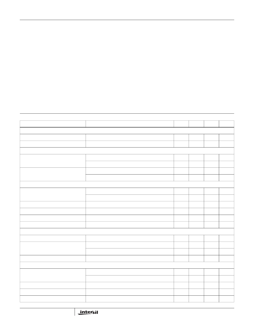
Electrical Specifications
Operating Conditions: VCC = 5V, T
A
= -10°C to 100°C. Unless Otherwise Specified.
PARAMETER
TEST CONDITIONS
MIN
TYP
MAX
UNITS
VCC SUPPLY CURRENT
Nominal Supply
VCC = 5VDC; EN = 5VDC; R
T
= 100k
±1%
8.0
10.8
14.0
mA
Shutdown Supply
VCC = 5VDC; EN = 0VDC; R
T
= 100k
±1%
8.0
10.3
13.0
mA
POWER-ON RESET AND ENABLE
POR Threshold
VCC Rising
4.25
4.35
4.60
V
VCC Falling
3.75
3.85
4.00
V
ENABLE Threshold
EN Rising
1.215
1.240
1.265
V
Hysteresis
82
92
102
mV
REFERENCE VOLTAGE AND DAC
System Accuracy (Note 5)
-1.2
-
1.2
%VID
0 to 70°C
-1
-
1
%VID
VID on Fly Step Size
R
T
= 100k
-
25
-
mV
VID Pull Up
-30
-20
-10
μ
A
VID Input Low Level
-
-
0.8
V
VID Input High Level
2.0
-
-
V
PIN-ADJUSTABLE OFFSET
OFS Current
-
100
-
μ
A
Offset Accuracy
ROFS = 5k
±
1%
92.0
100.0
108.0
mV
ROFS = 5k
±1% ,
0 to 70°C
94.0
100.0
106.0
Maximum Offset
-
-
100.0
mV
OSCILLATOR
Accuracy
-12.5
-
12.5
%
RT = 100K
245
280
315
kHz
Adjustment Range
0.08
-
1.0
MHz
VFF Range
0.5
-
2.5
V
Max Duty Cycle
-
75
-
%
ISL6244
相關PDF資料 |
PDF描述 |
|---|---|
| ISL6244HRZ | Multi-Phase PWM Controller |
| ISL6244HRZ-T | Multi-Phase PWM Controller |
| ISL6244 | Multi-Phase PWM Controller(多相PWM控制器) |
| ISL6244CRZ | Octal D-Type Transparent Latches With 3-State Outputs 20-PDIP -40 to 85 |
| ISL6244CRZ-T | Octal D-Type Transparent Latches With 3-State Outputs 20-SO -40 to 85 |
相關代理商/技術參數(shù) |
參數(shù)描述 |
|---|---|
| ISL6244HRZ | 功能描述:電流型 PWM 控制器 VER OF ISL6244HR RoHS:否 制造商:Texas Instruments 開關頻率:27 KHz 上升時間: 下降時間: 工作電源電壓:6 V to 15 V 工作電源電流:1.5 mA 輸出端數(shù)量:1 最大工作溫度:+ 105 C 安裝風格:SMD/SMT 封裝 / 箱體:TSSOP-14 |
| ISL6244HRZ-T | 功能描述:電流型 PWM 控制器 VER OF ISL6244HR-T RoHS:否 制造商:Texas Instruments 開關頻率:27 KHz 上升時間: 下降時間: 工作電源電壓:6 V to 15 V 工作電源電流:1.5 mA 輸出端數(shù)量:1 最大工作溫度:+ 105 C 安裝風格:SMD/SMT 封裝 / 箱體:TSSOP-14 |
| ISL6246C WAF | 制造商:Intersil Corporation 功能描述: |
| ISL6247 6248 WAF | 制造商:Intersil Corporation 功能描述: |
| ISL6247ACR-T | 制造商:Rochester Electronics LLC 功能描述:- Tape and Reel 制造商:Intersil Corporation 功能描述: |
發(fā)布緊急采購,3分鐘左右您將得到回復。