- 您現(xiàn)在的位置:買賣IC網(wǎng) > PDF目錄383145 > ISL6308CRZ (INTERSIL CORP) Three-Phase Buck PWM Controller with High Current Integrated MOSFET Drivers PDF資料下載
參數(shù)資料
| 型號: | ISL6308CRZ |
| 廠商: | INTERSIL CORP |
| 元件分類: | 穩(wěn)壓器 |
| 英文描述: | Three-Phase Buck PWM Controller with High Current Integrated MOSFET Drivers |
| 中文描述: | SWITCHING CONTROLLER, 1500 kHz SWITCHING FREQ-MAX, PQCC40 |
| 封裝: | 6 X 6 MM, ROHS COMPLIANT, PLASTIC, MO-220VJJD-1, QFN-40 |
| 文件頁數(shù): | 21/27頁 |
| 文件大小: | 765K |
| 代理商: | ISL6308CRZ |
第1頁第2頁第3頁第4頁第5頁第6頁第7頁第8頁第9頁第10頁第11頁第12頁第13頁第14頁第15頁第16頁第17頁第18頁第19頁第20頁當(dāng)前第21頁第22頁第23頁第24頁第25頁第26頁第27頁
21
FN9208.2
October 19, 2005
Since the system poles and zero are affected by the values
of the components that are meant to compensate them, the
solution to the system equation becomes fairly complicated.
Fortunately, there is a simple approximation that comes very
close to an optimal solution. Treating the system as though it
were a voltage-mode regulator, by compensating the L-C
poles and the ESR zero of the voltage mode approximation,
yields a solution that is always stable with very close to ideal
transient performance.
The feedback resistor, R
1
, has already been chosen as
outlined in
Load-Line Regulation Resistor.
Select a target
bandwidth for the compensated system, F
0
. The target
bandwidth must be large enough to assure adequate
transient performance, but smaller than 1/3 of the per-
channel switching frequency. The values of the
compensation components depend on the relationships of
F
0
to the L-C double pole frequency and the ESR zero
frequency. For each of the following three, there is a
separate set of equations for the compensation components.
In Equations 28, L is the per-channel filter inductance
divided by the number of active channels; C is the sum total
of all output capacitors; ESR is the equivalent series
resistance of the bulk output filter capacitance; and V
PP
is
the peak-to-peak sawtooth signal amplitude as described in
the
Electrical Specifications
.
Once selected, the compensation values in Equations 28
assure a stable converter with reasonable transient
performance. In most cases, transient performance can be
improved by making adjustments to R
2
. Slowly increase the
value of R
2
while observing the transient performance on an
oscilloscope until no further improvement is noted. Normally,
C
1
will not need adjustment. Keep the value of C
1
from
Equations 28 unless some performance issue is noted.
The optional capacitor C
2
, is sometimes needed to bypass
noise away from the PWM comparator (see Figure 19). Keep
a position available for C
2
, and be prepared to install a high
frequency capacitor of between 22pF and 150pF in case any
leading edge jitter problem is noted.
Compensating the Converter operating without
Load-Line Regulation
The ISL6308 multi-phase converter operating without load
line regulation behaves in a similar manner to a voltage-
mode controller. This section highlights the design
consideration for a voltage-mode controller requiring external
compensation. To address a broad range of applications, a
type-3 feedback network is recommended (see Figure 20).
Figure 21 highlights the voltage-mode control loop for a
synchronous-rectified buck converter, applicable, with a
small number of adjustments, to the multi-phase ISL6308
circuit. The output voltage (V
OUT
) is regulated to the reference
voltage, VREF, level. The error amplifier output (COMP pin
voltage) is compared with the oscillator (OSC) modified saw-
tooth wave to provide a pulse-width modulated wave with an
amplitude of V
IN
at the PHASE node. The PWM wave is
smoothed by the output filter (L and C). The output filter
capacitor bank’s equivalent series resistance is represented by
the series resistor E.
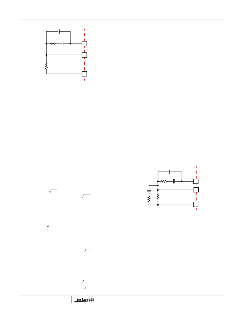
FIGURE 19. COMPENSATION CONFIGURATION FOR
LOAD-LINE REGULATED ISL6308 CIRCUIT
ISL6308
COMP
C
1
R
2
R
1
FB
VDIFF
C
2
(Optional)
2
π
L C
-----------1
F
0
>
R
2
R
1
2
π
F
V
IN
0.66 V
π
V
OSC
R
1
f
0
L C
-----------------0.66 V
=
C
1
2
=
Case 1:
2
π
L C
-----------1
F
0
π
C ESR
2
<
≤
R
2
R
1
V
-------------------0.66 V
2
π
(
)
2
F
2
L C
IN
0.66 V
=
C
1
2
π
(
)
F
0
V
OSC
R
1
L C
-------------------------------------------------------------------------------
=
Case 2:
(EQ. 28)
F
0
π
C ESR
2
>
R
2
R
1
2
π
F
V
L
0.66 V
IN
ESR
-----------------------------------------------
=
C
2
0.66 V
ESR
2
π
V
OSC
R
1
F
0
L
------------------------------------------------------C
=
Case 3:
FIGURE 20. COMPENSATION CONFIGURATION FOR
NON-LOAD-LINE REGULATED ISL6308 CIRCUIT
ISL6308
COMP
C
1
R
2
R
1
FB
VDIFF
C
2
R
3
C
3
ISL6308
相關(guān)PDF資料 |
PDF描述 |
|---|---|
| ISL6308CRZ-T | Quadruple 2-Input Exclusive-OR Gates 14-SOIC -40 to 85 |
| ISL6308IRZ-T | Three-Phase Buck PWM Controller with High Current Integrated MOSFET Drivers |
| ISL6315 | Two-Phase Multiphase Buck PWM Controller with Integrated MOSFET Drivers(帶集成MOSFET驅(qū)動器的雙相降壓PWM控制器) |
| ISL6316 | Quadruple 2-Input Exclusive-OR Gates 14-SOIC -40 to 85 |
| ISL6316IRZ | MINIATURE TOGGLE SWITCH |
相關(guān)代理商/技術(shù)參數(shù) |
參數(shù)描述 |
|---|---|
| ISL6308CRZR5374 | 制造商:Intersil Corporation 功能描述:ISL6308CRZ W/ 24HR BURN-IN - Rail/Tube 制造商:Intersil Corporation 功能描述:IC CTRLR PWM 3PHASE BUCK 40-QFN 制造商:Intersil 功能描述:ISL6308CRZ W/24HRU RN-IN |
| ISL6308CRZ-T | 功能描述:電壓模式 PWM 控制器 DAC-LESS MULTI-PHS PWM CNTRLR W/3-DRVRS RoHS:否 制造商:Texas Instruments 輸出端數(shù)量:1 拓?fù)浣Y(jié)構(gòu):Buck 輸出電壓:34 V 輸出電流: 開關(guān)頻率: 工作電源電壓:4.5 V to 5.5 V 電源電流:600 uA 最大工作溫度:+ 125 C 最小工作溫度:- 40 C 封裝 / 箱體:WSON-8 封裝:Reel |
| ISL6308CRZ-TR5374 | 制造商:Intersil Corporation 功能描述:ISL6308CRZ W/ 24HR BURN-IN - Tape and Reel 制造商:Intersil Corporation 功能描述:IC CTRLR PWM 3PHASE BUCK 40-QFN 制造商:Intersil 功能描述:ISL6308CRZ W/24HRU RN-IN |
| ISL6308CRZ-TR5453 | 制造商:Intersil Corporation 功能描述:STD. ISL6308CRZ-T W/GOLD BOND WIRE ONLY - Tape and Reel |
| ISL6308EVAL1Z | 制造商:Intersil Corporation 功能描述:ISL6308 EVALUATION BOARD 1 - ROHS COMPLIANT - QFN - Bulk |
發(fā)布緊急采購,3分鐘左右您將得到回復(fù)。