- 您現(xiàn)在的位置:買賣IC網(wǎng) > PDF目錄384525 > ISL6431A (Intersil Corporation) Advanced Pulse Width Modulation (PWM) Controller for Broadband Applications PDF資料下載
參數(shù)資料
| 型號: | ISL6431A |
| 廠商: | Intersil Corporation |
| 英文描述: | Advanced Pulse Width Modulation (PWM) Controller for Broadband Applications |
| 中文描述: | 先進的脈沖寬度調(diào)制(PWM)控制器的寬帶應用 |
| 文件頁數(shù): | 6/10頁 |
| 文件大小: | 215K |
| 代理商: | ISL6431A |
6
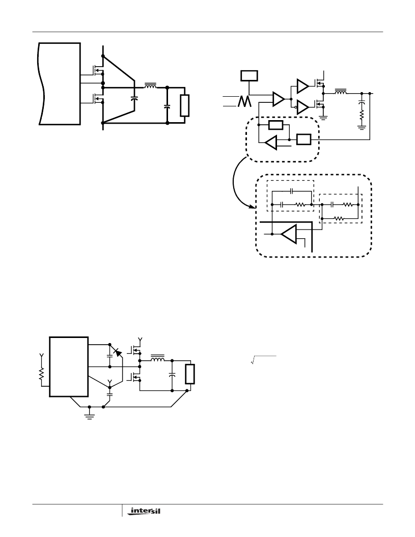
Figure 3 shows the critical power components of the converter.
To minimize the voltage overshoot, the interconnecting wires
indicated by heavy lines should be part of a ground or power
plane in a printed circuit board. The components shown in
Figure 3 should be located as close together as possible.
Please note that the capacitors C
IN
and C
O
may each
represent numerous physical capacitors. Locate the
ISL6431A
within 3 inches of the MOSFETs, Q
1
and Q
2
. The circuit traces
for the MOSFETs’ gate and source connections from the
ISL6431A must be sized to handle up to 1A peak current.
Figure 4 shows the circuit traces that require additional
layout consideration. Use single point and ground plane
construction for the circuits shown. Minimize any leakage
current paths on the COMP/OCSET pin and locate the
resistor, R
OSCET
close to the COMP/OCSET pin because
the internal current source is only 20
μ
A. Provide local V
CC
decoupling between VCC and GND pins. Locate the
capacitor, C
BOOT
as close as practical to the BOOT and
PHASE pins. All components used for feedback
compensation should be located as close to the IC a
practical.
Feedback Compensation
Figure 5 highlights the voltage-mode control loop for a
synchronous-rectified buck converter. The output voltage
(V
OUT
) is regulated to the Reference voltage level. The
error amplifier (Error Amp) output (V
E/A
) is compared with
the oscillator (OSC) triangular wave to provide a
pulse-width modulated (PWM) wave with an amplitude of
V
IN
at the PHASE node. The PWM wave is smoothed by the
output filter (L
O
and C
O
).
The modulator transfer function is the small-signal transfer
function of V
OUT
/V
E/A
. This function is dominated by a DC
Gain and the output filter (L
O
and C
O
), with a double pole
break frequency at F
LC
and a zero at F
ESR
. The DC Gain of
the modulator is simply the input voltage (V
IN
) divided by the
peak-to-peak oscillator voltage
V
OSC
.
Modulator Break Frequency Equations
The compensation network consists of the error amplifier
(internal to the ISL6431A) and the impedance networks Z
IN
and Z
FB
. The goal of the compensation network is to provide
a closed loop transfer function with the highest 0dB crossing
frequency (f
0dB
) and adequate phase margin. Phase margin
is the difference between the closed loop phase at f
0dB
and
180 degrees. The equations below relate the compensation
network’s poles, zeros and gain to the components (R
1
, R
2
,
R
3
, C
1
, C
2
, and C
3
) in Figure 7. Use these guidelines for
locating the poles and zeros of the compensation network:
1. Pick Gain (R
2
/R
1
) for desired converter bandwidth.
2. Place 1
ST
Zero Below Filter’s Double Pole (~75% F
LC
).
3. Place 2
ND
Zero at Filter’s Double Pole.
4. Place 1
ST
Pole at the ESR Zero.
L
O
C
O
LGATE
UGATE
PHASE
Q
1
Q
2
V
IN
V
OUT
RETURN
ISL6431A
C
IN
L
FIGURE 3. PRINTED CIRCUIT BOARD POWER AND
GROUND PLANES OR ISLANDS
FIGURE 4. PRINTED CIRCUIT BOARD SMALL SIGNAL
LAYOUT GUIDELINES
+5V
ISL6431A
COMP/OCSET
GND
VCC
BOOT
D
1
L
O
C
O
V
OUT
L
Q
1
Q
2
PHASE
+V
IN
C
BOOT
C
VCC
R
O
+5V
FIGURE 5. VOLTAGE-MODE BUCK CONVERTER
COMPENSATION DESIGN
V
OUT
REFERENCE
L
O
C
O
ESR
V
IN
V
OSC
ERROR
AMP
PWM
DRIVER
(PARASITIC)
Z
FB
+
-
REFERENCE
R
1
R
3
R
2
C
3
C
2
C
1
COMP
V
OUT
FB
Z
FB
ISL6431A
Z
IN
COMPARATOR
DRIVER
DETAILED COMPENSATION COMPONENTS
PHASE
V
E/A
+
-
+
-
Z
IN
OSC
FLC
2
π
x LO x CO
--------------------1
=
FESR
π
x ESR x CO
2
=
ISL6431A
相關PDF資料 |
PDF描述 |
|---|---|
| ISL6431ACB | Advanced Pulse Width Modulation (PWM) Controller for Broadband Applications |
| ISL6520A | Adjustable Precision Shunt Regulator 3-SOT-23 -40 to 125 |
| ISL6525CBZ | Buck and Synchronous-Rectifier Pulse-Width Modulator (PWM) Controller |
| ISL6525 | Adjustable Precision Shunt Regulator 5-SOT-23 -40 to 125 |
| ISL6525CB | Buck and Synchronous-Rectifier Pulse-Width Modulator (PWM) Controller |
相關代理商/技術參數(shù) |
參數(shù)描述 |
|---|---|
| ISL6431ACB | 制造商:Rochester Electronics LLC 功能描述:- Bulk |
| ISL6431CB | 功能描述:電壓模式 PWM 控制器 For Home Gateways RoHS:否 制造商:Texas Instruments 輸出端數(shù)量:1 拓撲結構:Buck 輸出電壓:34 V 輸出電流: 開關頻率: 工作電源電壓:4.5 V to 5.5 V 電源電流:600 uA 最大工作溫度:+ 125 C 最小工作溫度:- 40 C 封裝 / 箱體:WSON-8 封裝:Reel |
| ISL6431CB-T | 功能描述:IC REG CTRLR BUCK PWM VM 8-SOIC RoHS:否 類別:集成電路 (IC) >> PMIC - 穩(wěn)壓器 - DC DC 切換控制器 系列:- 標準包裝:4,000 系列:- PWM 型:電壓模式 輸出數(shù):1 頻率 - 最大:1.5MHz 占空比:66.7% 電源電壓:4.75 V ~ 5.25 V 降壓:是 升壓:無 回掃:無 反相:無 倍增器:無 除法器:無 Cuk:無 隔離:無 工作溫度:-40°C ~ 85°C 封裝/外殼:40-VFQFN 裸露焊盤 包裝:帶卷 (TR) |
| ISL6431IB | 制造商:Intersil Corporation 功能描述: |
| ISL6432CB | 制造商:Intersil Corporation 功能描述: |
發(fā)布緊急采購,3分鐘左右您將得到回復。