3
FN8226.1
September 18, 2006
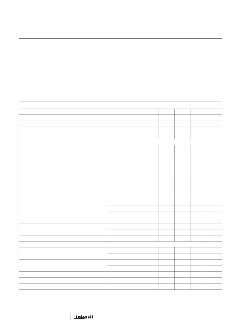
Absolute Maximum Ratings
Thermal Information
Temperature Under Bias . . . . . . . . . . . . . . . . . . . . -40 C to +85 C
Voltage on Any Pin with Respect to GND . . . . . . . . . . .-1.0V to +7V
D.C. Output Current. . . . . . . . . . . . . . . . . . . . . . . . . . . . . . . . . . 5mA
Recommended
Operating Conditions
Industrial . . . . . . . . . . . . . . . . . . . . . . . . . . . . . . . . . .-40°C to +85°C
Thermal Resistance (Typical, Note 1)
MSOP Package . . . . . . . . . . . . . . . . . . . . . . . . . . . .
Maximum Junction Temperature (Plastic Package) . . . . . . .+150°C
Maximum Storage Temperature Range. . . . . . . . . .-65°C to +150°C
Maximum Lead Temperature (Soldering 10s) . . . . . . . . . . . .+300°C
(MSOP - Lead Tips Only)
θ
JA
(°C/W)
145
CAUTION: Stresses above those listed in “Absolute Maximum Ratings” may cause permanent damage to the device. This is a stress only rating and operation of the
device at these or any other conditions above those indicated in the operational sections of this specification is not implied.
NOTE:
1.
θ
JA
is measured with the component mounted on a high effective thermal conductivity test board in free air. See Tech Brief TB379 for details.
Electrical Specifications
Over the recommended operating conditions unless otherwise specified.
SYMBOL
PARAMETER
TEST CONDITIONS
MIN
TYP
MAX
UNITS
V
DD
Supply Voltage Range
2.0
5.5
V
I
DD1
V
DD
Supply Current
V
DD
= 5.0V
12.5
15
μA
I
DD2
V2MON Input Current
V2MON = 3.3V
5.5
6
μA
I
DDA
V3MON Input Current
V3MON = 1.0V
19
100
nA
VOLTAGE THRESHOLDS
V
TH1
Fixed Voltage Trip Point for V
DD
ISL88021/22IU8
H
xZ
4.565
4.649
4.733
V
ISL88021/22IU8
F
xZ
3.029
3.085
3.141
V
V
TH1HYST
Hysteresis of V
TH1
V
TH1
= 4.64V
46
mV
V
TH1
= 3.09V
37
mV
V
TH2
Fixed Voltage Trip Point for V2MON
ISL88021/22IU8x
F
Z
3.034
3.090
3.146
V
ISL88021/22IU8x
E
Z
2.894
2.947
3.000
V
ISL88021/22IU8x
C
Z
2.290
2.332
2.374
V
ISL88021/22IU8x
A
Z
1.660
1.690
1.720
V
V
TH2HYST
Hysteresis of V
TH2
V
TH2
= 3.09V
37
mV
V
TH2
= 2.92V
29
mV
V
TH2
= 2.32V
23
mV
V
TH2
= 2.19V
22
mV
V
TH2
= 1.69V
17
mV
V
TH3
V3MON Threshold Voltage
V
TH
for V3MON on ISL88021
0.594
0.605
0.616
V
V
TH
for V3MON on ISL88022
0.587
0.595
0.603
V
V
REFHYST
Hysteresis Voltage
3
mV
RESET
V
OL
Reset Output Voltage Low
V
DD
≥
3.3V, Sinking 2.5mA
0.05
0.40
V
V
DD
< 3.3V, Sinking 1.5mA
V
DD
≥
3.3V, Sourcing 2.5mA
0.05
0.40
V
V
OH
RST Output Voltage High
V
DD
-0.6
V
DD
-0.4
V
V
DD
< 3.3V, Sourcing 1.5mA
V
DD
-0.6
V
DD
-0.4
V
t
RPD
V
TH
to Reset Asserted Delay
10
μs
t
POR
POR Timeout Delay
C
POR
is open
140
200
ms
C
LOAD
Load Capacitance on Reset Pins
5
pF
ISL88021, ISL88022