- 您現(xiàn)在的位置:買賣IC網(wǎng) > PDF目錄383173 > ISL8840AAUZ (INTERSIL CORP) High Performance Industry Standard Single-Ended Current Mode PWM Controller PDF資料下載
參數(shù)資料
| 型號(hào): | ISL8840AAUZ |
| 廠商: | INTERSIL CORP |
| 元件分類: | 穩(wěn)壓器 |
| 英文描述: | High Performance Industry Standard Single-Ended Current Mode PWM Controller |
| 中文描述: | 1 A SWITCHING REGULATOR, 2000 kHz SWITCHING FREQ-MAX, PDSO8 |
| 封裝: | ROHS COMPLIANT, PLASTIC, MO-187AA, MSOP-8 |
| 文件頁數(shù): | 11/15頁 |
| 文件大?。?/td> | 313K |
| 代理商: | ISL8840AAUZ |
11
FN6320.3
April 18, 2007
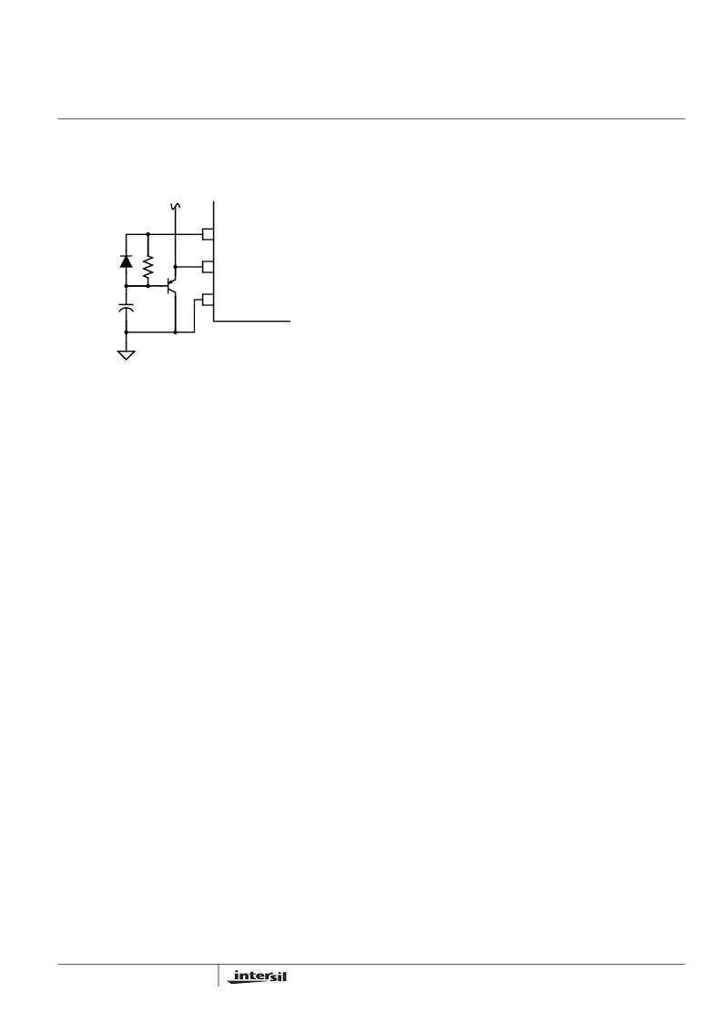
Soft-Start Operation
Soft-start must be implemented externally. One method,
illustrated below, clamps the voltage on COMP.
The COMP pin is clamped to the voltage on capacitor C1
plus a base-emitter junction by transistor Q1. C1 is charged
from VREF through resistor R1 and the base current of Q1.
At power-up C1 is fully discharged, COMP is at ~0.7V, and
the duty cycle is zero. As C1 charges, the voltage on COMP
increases, and the duty cycle increases in proportion to the
voltage on C1. When COMP reaches the steady state
operating point, the control loop takes over and soft start is
complete. C1 continues to charge up to VREF and no longer
affects COMP. During power down, diode D1 quickly
discharges C1 so that the soft start circuit is properly
initialized prior to the next power on sequence.
Gate Drive
The ISL884xA is capable of sourcing and sinking 1A peak
current. To limit the peak current through the IC, an optional
external resistor may be placed between the totem-pole
output of the IC (OUT pin) and the gate of the MOSFET. This
small series resistor also damps any oscillations caused by
the resonant tank of the parasitic inductances in the traces of
the board and the FET’s input capacitance.
Slope Compensation
For applications where the maximum duty cycle is less than
50%, slope compensation may be used to improve noise
immunity, particularly at lighter loads. The amount of slope
compensation required for noise immunity is determined
empirically, but is generally about 10% of the full scale
current feedback signal. For applications where the duty
cycle is greater than 50%, slope compensation is required to
prevent instability.
Slope compensation may be accomplished by summing an
external ramp with the current feedback signal or by
subtracting the external ramp from the voltage feedback
error signal. Adding the external ramp to the current
feedback signal is the more popular method.
From the small signal current-mode model [1] it can be
shown that the naturally-sampled modulator gain, Fm,
without slope compensation, is in Equation 6.
where Sn is the slope of the sawtooth signal and Tsw is the
duration of the half-cycle. When an external ramp is added,
the modulator gain becomes:
where Se is slope of the external ramp and
The criteria for determining the correct amount of external
ramp can be determined by appropriately setting the
damping factor of the double-pole located at the switching
frequency. The double-pole will be critically damped if the
Q-factor is set to 1, over-damped for Q < 1, and
under-damped for Q > 1. An under-damped condition may
result in current loop instability.
where D is the percent of on time during a switching cycle.
Setting Q = 1 and solving for Se yields
Since Sn and Se are the on time slopes of the current ramp
and the external ramp, respectively, they can be multiplied
by t
ON
to obtain the voltage change that occurs during t
ON
.
where Vn is the change in the current feedback signal (
Δ
I)
during the on time and Ve is the voltage that must be added
by the external ramp.
For a flyback converter, Vn can be solved for in terms of
input voltage, current transducer components, and primary
inductance, yielding
where R
CS
is the current sense resistor, f
sw
is the switching
frequency, L
p
is the primary inductance, V
IN
is the minimum
input voltage, and D is the maximum duty cycle.
FIGURE 5. SOFT-START
VREF
COMP
GND
I
C1
Q1
D1
R1
Fm
-------------------
=
(EQ. 6)
Fm
+
(
)
Tsw
--------------------------------------
c
---------------------------
=
=
(EQ. 7)
m
c
1
-------
+
=
(EQ. 8)
Q
–
π
m
c
1
D
(
)
0.5
–
(
)
-------------------------------------------------
=
(EQ. 9)
S
e
S
n
1
π
--
0.5
+
–
1
D
-------------
1
–
=
(EQ. 10)
V
e
V
n
1
π
--
0.5
+
–
1
D
-------------
1
–
=
(EQ. 11)
V
e
D T
----------------------------------------------------
V
R
p
1
π
--
0.5
+
D
---–
1
–
=
V
(EQ. 12)
ISL8840A, ISL8841A, ISL8842A, ISL8843A, ISL8844A, ISL8845A
相關(guān)PDF資料 |
PDF描述 |
|---|---|
| ISL8840AMBZ | High Performance Industry Standard Single-Ended Current Mode PWM Controller |
| ISL8840AMUZ | High Performance Industry Standard Single-Ended Current Mode PWM Controller |
| ISL8841A | High Performance Industry Standard Single-Ended Current Mode PWM Controller |
| ISL8841AABZ | High Performance Industry Standard Single-Ended Current Mode PWM Controller |
| ISL8841AAUZ | High Performance Industry Standard Single-Ended Current Mode PWM Controller |
相關(guān)代理商/技術(shù)參數(shù) |
參數(shù)描述 |
|---|---|
| ISL8840AAUZ-T | 功能描述:IC REG CTRLR BST FLYBK ISO 8MSOP RoHS:是 類別:集成電路 (IC) >> PMIC - 穩(wěn)壓器 - DC DC 切換控制器 系列:- 產(chǎn)品培訓(xùn)模塊:Lead (SnPb) Finish for COTS Obsolescence Mitigation Program 標(biāo)準(zhǔn)包裝:2,500 系列:- PWM 型:電流模式 輸出數(shù):1 頻率 - 最大:275kHz 占空比:50% 電源電壓:18 V ~ 110 V 降壓:無 升壓:無 回掃:無 反相:無 倍增器:無 除法器:無 Cuk:無 隔離:是 工作溫度:-40°C ~ 85°C 封裝/外殼:8-SOIC(0.154",3.90mm 寬) 包裝:帶卷 (TR) |
| ISL8840AMBEP | 制造商:Intersil Corporation 功能描述:CURRENT MODE PWM CNTRLR 1A 8SOIC N - Rail/Tube |
| ISL8840AMBEP-TK | 制造商:Intersil Corporation 功能描述:CURRENT MODE PWM CNTRLR 1A 8SOIC N - Tape and Reel |
| ISL8840AMBEPZ | 制造商:Intersil Corporation 功能描述:PB-FREE, -55 TO +125, CURRENT MODE PWM, 100% DC, 7.0V UVLO,8 - Rail/Tube |
| ISL8840AMBEPZ-TK | 制造商:Intersil Corporation 功能描述:PB-FREE,-55 TO+125,CURRENT MODE PWM, 100% DC,7.0V UVLO,8LD S - Tape and Reel |
發(fā)布緊急采購,3分鐘左右您將得到回復(fù)。