- 您現(xiàn)在的位置:買賣IC網(wǎng) > PDF目錄383173 > ISL8844AMBZ (INTERSIL CORP) High Performance Industry Standard Single-Ended Current Mode PWM Controller PDF資料下載
參數(shù)資料
| 型號: | ISL8844AMBZ |
| 廠商: | INTERSIL CORP |
| 元件分類: | 穩(wěn)壓器 |
| 英文描述: | High Performance Industry Standard Single-Ended Current Mode PWM Controller |
| 中文描述: | 1 A SWITCHING REGULATOR, 2000 kHz SWITCHING FREQ-MAX, PDSO8 |
| 封裝: | ROHS COMPLIANT, PLASTIC, MO-012AA, SOIC-8 |
| 文件頁數(shù): | 7/15頁 |
| 文件大小: | 313K |
| 代理商: | ISL8844AMBZ |
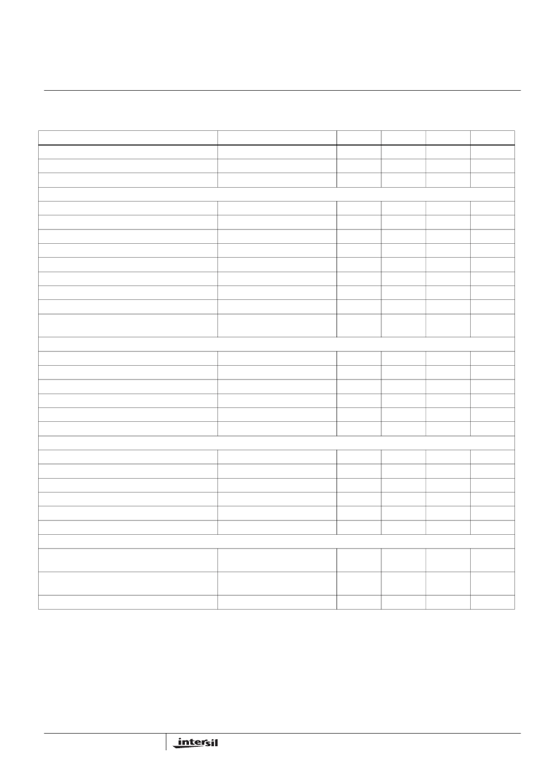
7
FN6320.3
April 18, 2007
Input Signal, Maximum
0.97
1.00
1.03
V
Gain, A
CS
=
Δ
V
COMP
/
Δ
V
CS
0 < V
CS
< 910mV, V
FB
= 0V
2.5
3.0
3.5
V/V
CS to OUT Delay
-
35
55
ns
ERROR AMPLIFIER
Open Loop Voltage Gain
(Note 5)
60
90
-
dB
Unity Gain Bandwidth
(Note 5)
1.0
1.5
-
MHz
Reference Voltage
V
FB
= V
COMP
2.475
2.500
2.530
V
FB Input Bias Current
V
FB
= 0V
-1.0
-0.2
1.0
μ
A
COMP Sink Current
V
COMP
= 1.5V, V
FB
= 2.7V
1.0
-
-
mA
COMP Source Current
V
COMP
= 1.5V, V
FB
= 2.3V
-0.4
-
-
mA
COMP VOH
V
FB
= 2.3V
4.80
-
VREF
V
COMP VOL
V
FB
= 2.7V
0.4
-
1.0
V
PSRR
Frequency = 120Hz, V
DD
= 12V to
30V (Note 5)
60
80
-
dB
OSCILLATOR
Frequency Accuracy
Initial, T
A
= +25°C
48
51
53
kHz
Frequency Variation with V
DD
T
A
= +25°C, (f
30V
- f
10V
)/f
30V
-
0.2
1.0
%
Temperature Stability
(Note 5)
-
-
5
%
Amplitude, Peak to Peak
Static Test
-
1.75
-
V
RTCT Discharge Voltage (Valley Voltage)
Static Test
-
1.0
-
V
Discharge Current
RTCT = 2.0V
6.5
7.8
8.5
mA
OUTPUT
Gate VOH
V
DD
to OUT, I
OUT
= -200mA
-
1.0
2.0
V
Gate VOL
OUT to GND, I
OUT
= 200mA
-
1.0
2.0
V
Peak Output Current
C
OUT
= 1nF (Note 5)
-
1.0
-
A
Rise Time
C
OUT
= 1nF (Note 5)
-
20
40
ns
Fall Time
C
OUT
= 1nF (Note 5)
-
20
40
ns
GATE VOL UVLO Clamp Voltage
VDD = 5V, I
LOAD
= 1mA
-
-
1.2
V
PWM
Maximum Duty Cycle
(ISL8840A, ISL8842A, ISL8843A)
COMP = VREF
94.0
96.0
-
%
Maximum Duty Cycle
(ISL8841A, ISL8844A, ISL8845A)
COMP = VREF
47.0
48.0
-
%
Minimum Duty Cycle
COMP = GND
-
-
0
%
NOTES:
3. Specifications at -40°C and +105°C are guaranteed by +25°C test with margin limits.
4. This is the V
DD
current consumed when the device is active but not switching. Does not include gate drive current.
5. These parameters, although guaranteed, are not 100% tested in production.
6. Adjust V
DD
above the start threshold and then lower to 15V.
Electrical Specifications
ISL884xAA -
Recommended operating conditions unless otherwise noted. Refer to Block Diagram and
Typical Application schematic onpage 3 and page 4. V
DD
= 15V, R
T
= 10k
Ω
, C
T
= 3.3nF,
T
A
= -40 to +105°C
(Note 3). Typical values are at T
A
= +25°C
(Continued)
PARAMETER
TEST CONDITIONS
MIN
TYP
MAX
UNITS
ISL8840A, ISL8841A, ISL8842A, ISL8843A, ISL8844A, ISL8845A
發(fā)布緊急采購,3分鐘左右您將得到回復(fù)。