- 您現(xiàn)在的位置:買賣IC網(wǎng) > PDF目錄373080 > K7A321800M-QC20 (SAMSUNG SEMICONDUCTOR CO. LTD.) 1Mx36 & 2Mx18 Synchronous SRAM PDF資料下載
參數(shù)資料
| 型號(hào): | K7A321800M-QC20 |
| 廠商: | SAMSUNG SEMICONDUCTOR CO. LTD. |
| 元件分類: | DRAM |
| 英文描述: | 1Mx36 & 2Mx18 Synchronous SRAM |
| 中文描述: | 1Mx36 |
| 文件頁數(shù): | 3/18頁 |
| 文件大?。?/td> | 247K |
| 代理商: | K7A321800M-QC20 |
1Mx36 & 2Mx18 Synchronous SRAM
- 3 -
Rev 2.0
Nov. 2003
K7A321800M
K7A323600M
1Mx36 & 2Mx18-Bit Synchronous Pipelined Burst SRAM
The K7A323600M and K7A321800M are 37,748,736-bit
Synchronous Static Random Access Memory designed for
high performance second level cache of Pentium and
Power PC based System.
It is organized as 1M(2M) words of 36(18) bits and inte-
grates address and control registers, a 2-bit burst address
counter and added some new functions for high perfor-
mance cache RAM applications; GW, BW, LBO, ZZ. Write
cycles are internally self-timed and synchronous.
Full bus-width write is done by GW, and each byte write is
performed by the combination of WEx and BW when GW is
high. And with CS
1
high, ADSP is blocked to control sig-
nals.
Burst cycle can be initiated with either the address status
processor(ADSP) or address status cache control-
ler(ADSC) inputs. Subsequent burst addresses are gener-
ated internally in the system
′
s burst sequence and are
controlled by the burst address advance(ADV) input.
LBO pin is DC operated and determines burst
sequence(linear or interleaved).
ZZ pin controls Power Down State and reduces Stand-by
current regardless of CLK.
The K7A323600M and K7A321800M are fabricated using
SAMSUNG
′
s high performance CMOS technology and is
available in a 100pin TQFP package. Multiple power and
ground pins are utilized to minimize ground bounce.
GENERAL DESCRIPTION
FEATURES
Synchronous Operation.
2 Stage Pipelined operation with 4 Burst.
On-Chip Address Counter.
Self-Timed Write Cycle.
On-Chip Address and Control Registers.
V
DD
= 3.3V +0.165V/-0.165V Power Supply.
I/O Supply Voltage 3.3V +0.165V/-0.165V for 3.3V I/O
or 2.5V+0.4V/-0.125V for 2.5V I/O.
5V Tolerant Inputs Except I/O Pins.
Byte Writable Function.
Global Write Enable Controls a full bus-width write.
Power Down State via ZZ Signal.
LBO Pin allows a choice of either a interleaved burst or a linear
burst.
Three Chip Enables for simple depth expansion with No Data Con-
tention only for TQFP ; 2cycle Enable, 1cycle Disable.
Asynchronous Output Enable Control.
ADSP, ADSC, ADV Burst Control Pins.
TTL-Level Three-State Output.
100-TQFP-1420A Package
Operating in commeical and industrial temperature range.
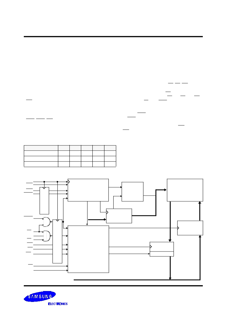
LOGIC BLOCK DIAGRAM
CLK
LBO
ADV
ADSC
ADSP
CS
1
CS
2
CS
2
GW
BW
WEx
(x=a,b,c,d or a,b)
OE
ZZ
DQa
~ DQd
or DQa0 ~ DQb7
DQPa ~ DQPd
BURST CONTROL
LOGIC
BURST
ADDRESS
COUNTER
1Mx36 , 2Mx18
MEMORY
ARRAY
ADDRESS
REGISTER
CONTROL
LOGIC
OUTPUT
REGISTER
DATA-IN
REGISTER
BUFFER
C
R
C
R
A
′
0
~A
′
1
A
0
~A
1
or A
2
~A
20
or A
0
~A
20
FAST ACCESS TIMES
PARAMETER
Symbol
-25
-20
-14
Unit
Cycle Time
tCYC
4.0
5.0
7.2
ns
Clock Access Time
tCD
2.6
3.1
4.0
ns
Output Enable Access Time
tOE
2.6
3.1
4.0
ns
A
0
~A
19
A
2
~A
19
DQPa,DQPb
相關(guān)PDF資料 |
PDF描述 |
|---|---|
| K7A321800M-QC25 | 1Mx36 & 2Mx18 Synchronous SRAM |
| K7A323600M | 1Mx36 & 2Mx18 Synchronous SRAM |
| K7A323600M-QC14 | 1Mx36 & 2Mx18 Synchronous SRAM |
| K7A323600M-QC20 | 1Mx36 & 2Mx18 Synchronous SRAM |
| K7A323600M-QC25 | 1Mx36 & 2Mx18 Synchronous SRAM |
相關(guān)代理商/技術(shù)參數(shù) |
參數(shù)描述 |
|---|---|
| K7A321800M-QC25 | 制造商:SAMSUNG 制造商全稱:Samsung semiconductor 功能描述:1Mx36 & 2Mx18 Synchronous SRAM |
| K7A321830C | 制造商:SAMSUNG 制造商全稱:Samsung semiconductor 功能描述:1Mx36 and 2Mx18 Synchronous SRAM |
| K7A321830C-PC20 | 制造商:SAMSUNG 制造商全稱:Samsung semiconductor 功能描述:1Mx36 and 2Mx18 Synchronous SRAM |
| K7A321830C-PI20 | 制造商:SAMSUNG 制造商全稱:Samsung semiconductor 功能描述:1Mx36 and 2Mx18 Synchronous SRAM |
| K7A321830C-QC20 | 制造商:SAMSUNG 制造商全稱:Samsung semiconductor 功能描述:1Mx36 and 2Mx18 Synchronous SRAM |
發(fā)布緊急采購,3分鐘左右您將得到回復(fù)。