- 您現(xiàn)在的位置:買賣IC網(wǎng) > PDF目錄373080 > K7B323625M (SAMSUNG SEMICONDUCTOR CO. LTD.) 1Mx36 & 2Mx18 Synchronous SRAM PDF資料下載
參數(shù)資料
| 型號: | K7B323625M |
| 廠商: | SAMSUNG SEMICONDUCTOR CO. LTD. |
| 元件分類: | DRAM |
| 英文描述: | 1Mx36 & 2Mx18 Synchronous SRAM |
| 中文描述: | 1Mx36 |
| 文件頁數(shù): | 6/19頁 |
| 文件大?。?/td> | 264K |
| 代理商: | K7B323625M |
K7B321825M
1Mx36 & 2Mx18 Synchronous SRAM
- 6 -
Rev 2.0
Nov. 2003
K7B323625M
FUNCTION DESCRIPTION
The K7B323625M and K7B321825M are synchronous SRAM designed to support the burst address accessing sequence of the
Power PC based microprocessor. All inputs (with the exception of OE, LBO and ZZ) are sampled on rising clock edges. The start and
duration of the burst access is controlled by ADSC, ADSP and ADV and chip select pins.
The accesses are enabled with the chip select signals and output enabled signals. Wait states are inserted into the access with
ADV.
When ZZ is pulled high, the SRAM will enter a Power Down State. At this time, internal state of the SRAM is preserved. When ZZ
returns to low, the SRAM normally operates after 2cycles of wake up time. ZZ pin is pulled down internally.
Read cycles are initiated with ADSP(or ADSC) using the new external address clocked into the on-chip address register when both
GW and BW are high or when BW is low and WEa, WEb, WEc, and WEd are high. When ADSP is sampled low, the chip selects are
sampled active, and the output buffer is enabled with OE. the data of cell array accessed by the current address are projected to the
output pins.
Write cycles are also initiated with ADSP(or ADSC) and are differentiated into two kinds of operations; All byte write operation and
individual byte write operation.
All byte write occurs by enabling GW(independent of BW and WEx.), and individual byte write is performed only when GW is high
and BW is low. In K7B163625M, a 512Kx36 organization, WEa controls DQa0 ~ DQa7 and DQPa, WEb controls DQb0 ~ DQb7 and
DQPb, WEc controls DQc0 ~ DQc7 and DQPc and WEd controls DQd0 ~ DQd7 and DQPd.
CS
1
is used to enable the device and conditions internal use of ADSP and is sampled only when a new external address is loaded.
ADV is ignored at the clock edge when ADSP is asserted, but can be sampled on the subsequent clock edges. The address
increases internally for the next access of the burst when ADV is sampled low.
Addresses are generated for the burst access as shown below, The starting point of the burst sequence is provided by the external
address. The burst address counter wraps around to its initial state upon completion. The burst sequence is determined by the state
of the LBO pin. When this pin is Low, linear burst sequence is selected. And this pin is High, Interleaved burst sequence is selected.
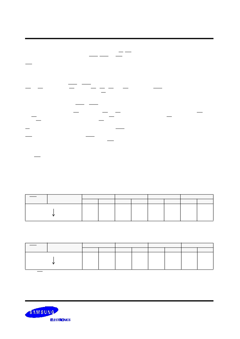
BURST SEQUENCE TABLE
(Interleaved Burst)
LBO PIN
HIGH
Case 1
Case 2
Case 3
Case 4
A
1
0
0
1
1
A
0
0
1
0
1
A
1
0
0
1
1
A
0
1
0
1
0
A
1
1
1
0
0
A
0
0
1
0
1
A
1
1
1
0
0
A
0
1
0
1
0
First Address
Fourth Address
BQ TABLE
(Linear Burst)
Note :
1. LBO pin must be tied to High or Low, and Floating State must not be allowed
.
LBO PIN
LOW
Case 1
Case 2
Case 3
Case 4
A
1
0
0
1
1
A
0
0
1
0
1
A
1
0
1
1
0
A
0
1
0
1
0
A
1
1
1
0
0
A
0
0
1
0
1
A
1
1
0
0
1
A
0
1
0
1
0
First Address
Fourth Address
相關(guān)PDF資料 |
PDF描述 |
|---|---|
| K7B323625M-QC75 | 1Mx36 & 2Mx18 Synchronous SRAM |
| K7A321800M | 1Mx36 & 2Mx18 Synchronous SRAM |
| K7A321800M-QC14 | 1Mx36 & 2Mx18 Synchronous SRAM |
| K7A321800M-QC20 | 1Mx36 & 2Mx18 Synchronous SRAM |
| K7A321800M-QC25 | 1Mx36 & 2Mx18 Synchronous SRAM |
相關(guān)代理商/技術(shù)參數(shù) |
參數(shù)描述 |
|---|---|
| K7B323625M-QC65 | 制造商:SAMSUNG 制造商全稱:Samsung semiconductor 功能描述:1Mx36 & 2Mx18 Synchronous SRAM |
| K7B323625M-QC6575 | 制造商:SAMSUNG 制造商全稱:Samsung semiconductor 功能描述:1Mx36 & 2Mx18 Synchronous SRAM |
| K7B323625M-QC75 | 制造商:SAMSUNG 制造商全稱:Samsung semiconductor 功能描述:1Mx36 & 2Mx18 Synchronous SRAM |
| K7B323635C | 制造商:SAMSUNG 制造商全稱:Samsung semiconductor 功能描述:1Mx36 & 2Mx18 Synchronous SRAM |
| K7B323635C-PI75000 | 制造商:Samsung SDI 功能描述: |
發(fā)布緊急采購,3分鐘左右您將得到回復(fù)。