- 您現(xiàn)在的位置:買賣IC網(wǎng) > PDF目錄373081 > K7I643684M-FI20 (SAMSUNG SEMICONDUCTOR CO. LTD.) 72Mb DDRII SRAM Specification PDF資料下載
參數(shù)資料
| 型號: | K7I643684M-FI20 |
| 廠商: | SAMSUNG SEMICONDUCTOR CO. LTD. |
| 英文描述: | 72Mb DDRII SRAM Specification |
| 中文描述: | 72Mb SRAM的規(guī)范條DDRII |
| 文件頁數(shù): | 10/18頁 |
| 文件大?。?/td> | 424K |
| 代理商: | K7I643684M-FI20 |
2Mx36 & 4Mx18 DDRII CIO b4 SRAM
K7I643684M
K7I641884M
- 10 -
Rev. 1.3 March 2007
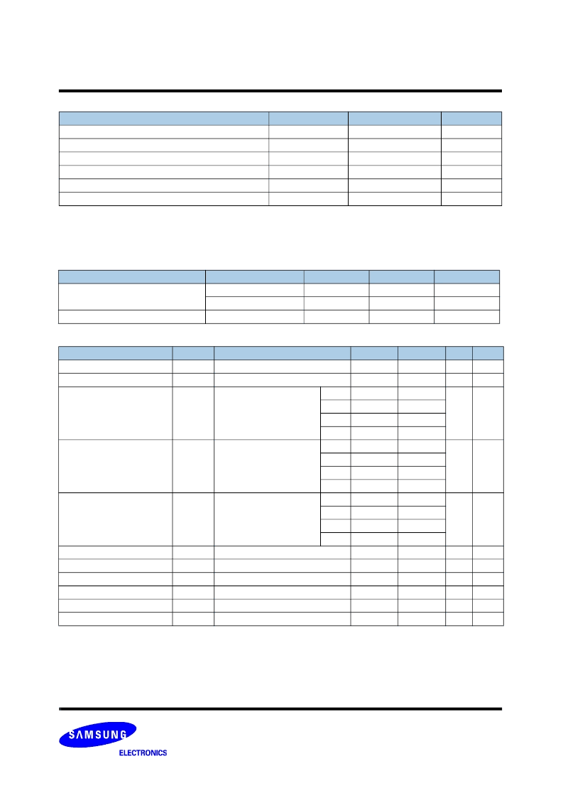
ABSOLUTE MAXIMUM RATINGS*
*Note:
1. Stresses greater than those listed under "Absolute Maximum Ratings" may cause permanent damage to the device. This is a stress rating
only and functional operation of the device at these or any other conditions above those indicated in the operating sections of this specification
is not implied. Exposure to absolute maximum rating conditions for extended periods may affect reliability.
2. V
DDQ
must not exceed V
DD
during normal operation.
PARAMETER
SYMBOL
RATING
UNIT
Voltage on V
DD
Supply Relative to V
SS
V
DD
-0.5 to 2.9
V
Voltage on V
DDQ
Supply Relative to V
SS
V
DDQ
-0.5 to V
DD
V
Voltage on Input Pin Relative to V
SS
V
IN
-0.5 to V
DD+
0.3
V
Storage Temperature
T
STG
-65 to 150
°
C
Operating Temperature (Commercial / Industrial)
T
OPR
0 to 70 / -40 to 85
°
C
Storage Temperature Range Under Bias
T
BIAS
-10 to 85
°
C
DC ELECTRICAL CHARACTERISTICS
(V
DD
=1.8V
±
0.1V, T
A
=0
°
C to +70
°
C)
Notes:
1. Minimum cycle. I
OUT
=0mA.
2. |I
OH
|=(V
DDQ
/2)/(RQ/5)
±
15% for 175
≤
RQ
≤
350
. |I
OL
|=(V
DDQ
/2)/(RQ/5)
±
15% for 175
≤
RQ
≤
350
.
3. Minimum Impedance Mode when ZQ pin is connected to V
DDQ
.
4. Operating current is calculated with 50% read cycles and 50% write cycles.
5. Standby Current is only after all pending read and write burst operations are completed.
6. Programmable Impedance Mode.
7. These are DC test criteria. DC design criteria is V
REF
±
50mV. The AC V
IH
/V
IL
levels are defined separately for measuring timing parameters.
8. V
IL
(Min)DC=
-
0.3V, V
IL
(Min)AC=-1.5V(pulse width
≤
3ns).
9. V
IH
(Max)DC=
V
DDQ
+0.3, V
IH
(Max)AC=
V
DDQ
+0.85V(pulse width
≤
3ns).
PARAMETER
SYMBOL
TEST CONDITIONS
MIN
MAX
UNIT
NOTES
Input Leakage Current
I
IL
V
DD
=Max ; V
IN
=V
SS
to V
DDQ
-2
+2
μ
A
Output Leakage Current
I
OL
Output Disabled,
-2
+2
μ
A
Operating Current (x36):
QDR mode
I
CC
V
DD
=Max, I
OUT
=0mA
Cycle Time
≥
t
KHKH
Min
-30
-
900
mA
1,4
-25
-
800
-20
-
700
-16
650
Operating Current (x18):
QDR mode
I
CC
V
DD
=Max, I
OUT
=0mA
Cycle Time
≥
t
KHKH
Min
-30
-
850
mA
1,4
-25
-
750
-20
-
650
-16
-
600
Standby Current(NOP):
QDR mode
I
SB1
Device deselected, I
OUT
=0mA,
f=Max,
All Inputs
≤
0.2V or
≥
V
DD
-0.2V
-30
-
400
mA
1,5
-25
-
380
-20
-
360
-16
-
340
Output High Voltage
V
OH1
V
DDQ
/2-0.12 V
DDQ
/2+0.12
V
2,6
Output Low Voltage
V
OL1
V
DDQ
/2-0.12 V
DDQ
/2+0.12
V
2,6
Output High Voltage
V
OH2
I
OH
=-1.0mA
V
DDQ
-0.2
V
DDQ
V
3
Output Low Voltage
V
OL2
I
OL
=1.0mA
V
SS
0.2
V
3
Input Low Voltage
V
IL
-0.3
V
REF
-0.1
V
7,8
Input High Voltage
V
IH
V
REF
+0.1
V
DDQ
+0.3
V
7,9
OPERATING CONDITIONS
(0
°
C
≤
T
A
≤
70
°
C)
PARAMETER
SYMBOL
MIN
MAX
UNIT
Supply Voltage
V
DD
1.7
1.9
V
V
DDQ
1.4
1.9
V
Reference
Voltage
V
REF
0.68
0.95
V
相關(guān)PDF資料 |
PDF描述 |
|---|---|
| K7I643684M-FI25 | 72Mb DDRII SRAM Specification |
| K7I643684M-FI30 | 72Mb DDRII SRAM Specification |
| K7M161835B-QC65 | 512Kx36 & 1Mx18 Pipelined NtRAM |
| K7N161831B | 512Kx36 & 1Mx18 Pipelined NtRAM |
| K7N163631B | 512Kx36 & 1Mx18 Pipelined NtRAM |
相關(guān)代理商/技術(shù)參數(shù) |
參數(shù)描述 |
|---|---|
| K7I643684M-FI25 | 制造商:SAMSUNG 制造商全稱:Samsung semiconductor 功能描述:72Mb DDRII SRAM Specification |
| K7I643684M-FI30 | 制造商:SAMSUNG 制造商全稱:Samsung semiconductor 功能描述:72Mb DDRII SRAM Specification |
| K7-J | 制造商:MITSUMI 制造商全稱:Mitsumi Electronics, Corp. 功能描述:Adjustable Type Coils |
| K7J161882B | 制造商:SAMSUNG 制造商全稱:Samsung semiconductor 功能描述:512Kx36 & 1Mx18 DDR II SIO b2 SRAM |
| K7J161882B-FC30000 | 制造商:Samsung SDI 功能描述:16MSYNC |
發(fā)布緊急采購,3分鐘左右您將得到回復(fù)。