- 您現(xiàn)在的位置:買賣IC網(wǎng) > PDF目錄373086 > K8D1716UTC-DI07 (SAMSUNG SEMICONDUCTOR CO. LTD.) 16M Bit (2M x8/1M x16) Dual Bank NOR Flash Memory PDF資料下載
參數(shù)資料
| 型號(hào): | K8D1716UTC-DI07 |
| 廠商: | SAMSUNG SEMICONDUCTOR CO. LTD. |
| 英文描述: | 16M Bit (2M x8/1M x16) Dual Bank NOR Flash Memory |
| 中文描述: | 1,600位(200萬x8/1M x16)的雙銀行NOR閃存 |
| 文件頁數(shù): | 23/41頁 |
| 文件大小: | 684K |
| 代理商: | K8D1716UTC-DI07 |
第1頁第2頁第3頁第4頁第5頁第6頁第7頁第8頁第9頁第10頁第11頁第12頁第13頁第14頁第15頁第16頁第17頁第18頁第19頁第20頁第21頁第22頁當(dāng)前第23頁第24頁第25頁第26頁第27頁第28頁第29頁第30頁第31頁第32頁第33頁第34頁第35頁第36頁第37頁第38頁第39頁第40頁第41頁
FLASH MEMORY
K8D1716UTC / K8D1716UBC
Revision 1.0
December 2004
23
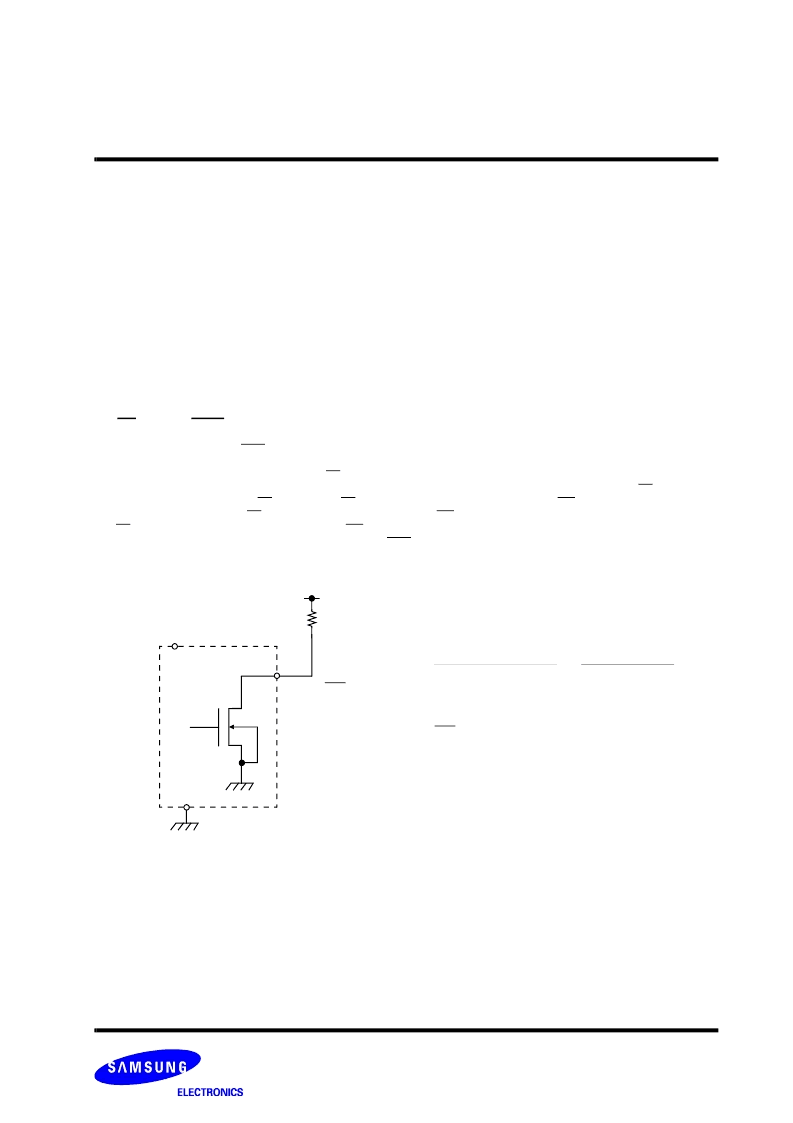
RY/BY : Ready/Busy
The K8D1716U has a Ready / Busy output that indicates either the completion of an operation or the status of Internal Algorithms. If
the output is Low, the device is busy with either a program or an erase operation. If the output is High, the device is ready to accept
any read/write or erase operation. When the RY/ BY pin is low, the device will not accept any additional program or erase commands
with the exception of the Erase Suspend command. If the K8D1716U is placed in an Erase Suspend mode, the RY/ BY output will be
High. For programming, the RY/ BY is valid (RY/ BY = 0) after the rising edge of the fourth WE pulse in the four write pulse
sequence. For Chip Erase, RY/ BY is also valid after the rising edge of WE pulse in the six write pulse sequence. For Block Erase,
RY/ BY is also valid after the rising edge of the sixth WE pulse.
The pin is an open drain output, allowing two or more Ready/ Busy outputs to be OR-tied. An appropriate pull-up resistor is required
for proper operation.
DQ3 : Block Erase Timer
The status of the multi-block erase operation can be detected via the DQ3 pin. DQ3 will go High if 50
μ
s of the block erase time win-
dow expires. In this case, the Internal Erase Routine will initiate the erase operation.Therefore, the device will not accept further write
commands until the erase operation is completed. DQ3 is Low if the block erase time window is not expired. Within the block erase
time window, an additional block erase command (30H) can be accepted. To confirm that the block erase command has been
accepted, the software may check the status of DQ3 following each block erase command.
DQ2 : Toggle Bit 2
The device generates a toggling pulse in DQ2 only if an Internal Erase Routine or an Erase Suspend is in progress. When the device
executes the Internal Erase Routine, DQ2 toggles only if an erasing block is read. Although the Internal Erase Routine is in the
Exceeded Time Limits, DQ2 toggles only if an erasing block in the Exceeded Time Limits is read. When the device is in the Erase
Suspend mode, DQ2 toggles only if an address in the erasing block is read. If a non-erasing block address is read during the Erase
Suspend mode, then DQ2 will produce valid data. DQ2 will go High if the user tries to program a non-erase suspend block while the
device is in the Erase Suspend mode. Combination of the status in DQ6 and DQ2 can be used to distinguish the erase operation
from the program operation.
Vcc
F
Ready / Busy
open drain output
Device
Vss
where
Σ
I
L
is the sum of the input currents of all devices tied to the
Ready / Busy ball.
Rp
Rp
=
Vcc
F
(Max.) - V
OL
(Max.)
I
OL
+
Σ
I
L
=
3.2V
2.1mA +
Σ
I
L
相關(guān)PDF資料 |
PDF描述 |
|---|---|
| K8D1716UTC-DI08 | 16M Bit (2M x8/1M x16) Dual Bank NOR Flash Memory |
| K8D1716UTC-DI09 | 16M Bit (2M x8/1M x16) Dual Bank NOR Flash Memory |
| K8D1716UTC-FC07 | 16M Bit (2M x8/1M x16) Dual Bank NOR Flash Memory |
| K8D1716UTC-FC08 | 16M Bit (2M x8/1M x16) Dual Bank NOR Flash Memory |
| K8D1716UTC-FC09 | 16M Bit (2M x8/1M x16) Dual Bank NOR Flash Memory |
相關(guān)代理商/技術(shù)參數(shù) |
參數(shù)描述 |
|---|---|
| K8D1716UTC-DI08 | 制造商:SAMSUNG 制造商全稱:Samsung semiconductor 功能描述:16M Bit (2M x8/1M x16) Dual Bank NOR Flash Memory |
| K8D1716UTC-DI09 | 制造商:SAMSUNG 制造商全稱:Samsung semiconductor 功能描述:16M Bit (2M x8/1M x16) Dual Bank NOR Flash Memory |
| K8D1716UTC-FC07 | 制造商:SAMSUNG 制造商全稱:Samsung semiconductor 功能描述:16M Bit (2M x8/1M x16) Dual Bank NOR Flash Memory |
| K8D1716UTC-FC08 | 制造商:SAMSUNG 制造商全稱:Samsung semiconductor 功能描述:16M Bit (2M x8/1M x16) Dual Bank NOR Flash Memory |
| K8D1716UTC-FC09 | 制造商:SAMSUNG 制造商全稱:Samsung semiconductor 功能描述:16M Bit (2M x8/1M x16) Dual Bank NOR Flash Memory |
發(fā)布緊急采購,3分鐘左右您將得到回復(fù)。