- 您現(xiàn)在的位置:買賣IC網(wǎng) > PDF目錄373086 > K8D1716UTC-DI09 (SAMSUNG SEMICONDUCTOR CO. LTD.) 16M Bit (2M x8/1M x16) Dual Bank NOR Flash Memory PDF資料下載
參數(shù)資料
| 型號(hào): | K8D1716UTC-DI09 |
| 廠商: | SAMSUNG SEMICONDUCTOR CO. LTD. |
| 英文描述: | 16M Bit (2M x8/1M x16) Dual Bank NOR Flash Memory |
| 中文描述: | 1,600位(200萬x8/1M x16)的雙銀行NOR閃存 |
| 文件頁(yè)數(shù): | 11/41頁(yè) |
| 文件大小: | 684K |
| 代理商: | K8D1716UTC-DI09 |
第1頁(yè)第2頁(yè)第3頁(yè)第4頁(yè)第5頁(yè)第6頁(yè)第7頁(yè)第8頁(yè)第9頁(yè)第10頁(yè)當(dāng)前第11頁(yè)第12頁(yè)第13頁(yè)第14頁(yè)第15頁(yè)第16頁(yè)第17頁(yè)第18頁(yè)第19頁(yè)第20頁(yè)第21頁(yè)第22頁(yè)第23頁(yè)第24頁(yè)第25頁(yè)第26頁(yè)第27頁(yè)第28頁(yè)第29頁(yè)第30頁(yè)第31頁(yè)第32頁(yè)第33頁(yè)第34頁(yè)第35頁(yè)第36頁(yè)第37頁(yè)第38頁(yè)第39頁(yè)第40頁(yè)第41頁(yè)
FLASH MEMORY
K8D1716UTC / K8D1716UBC
Revision 1.0
December 2004
11
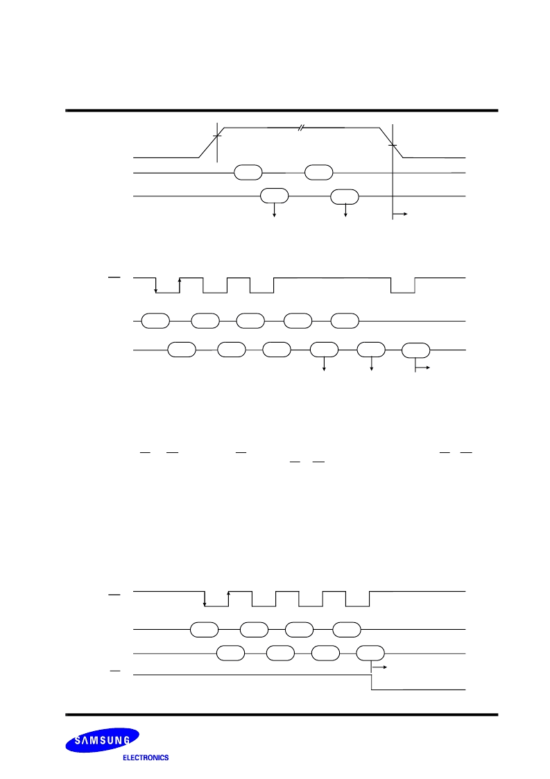
Figure 3. Autoselect Operation ( by command sequence method )
WE
555H/
AAAH
2AAH/
555H
555H/
AAAH
AAH
55H
90H
00H/
00H
01H/
02H
ECH
Manufacturer
Code
Device Code
(K8D1716U)
A19
~
A0(x16)/*
A19
~
A-1(x8)
DQ15
~
DQ0
F0H
Return to
Read Mode
Write (Program/Erase) Mode
The K8D1716U executes its program/erase operations by writing commands into the command register. In order to write the com-
mands to the register, CE and WE must be low and OE must be high. Addresses are latched on the falling edge of CE or WE (which-
ever occurs last) and the data are latched on the rising edge of CE or WE (whichever occurs first). The device uses standard
microprocessor write timing.
Program
The K8D1716U can be programmed in units of a word or a byte. Programming is writing 0's into the memory array by executing the
Internal Program Routine. In order to perform the Internal Program Routine, a four-cycle command sequence is necessary. The first
two cycles are unlock cycles. The third cycle is assigned for the program setup command. In the last cycle, the address of the mem-
ory location and the data to be programmed at that location are written. The device automatically generates adequate program
pulses and verifies the programmed cell margin by the Internal Program Routine. During the execution of the Routine, the system is
not required to provide further controls or timings.
During the Internal Program Routine, commands written to the device will be ignored. Note that a hardware reset during a program
operation will cause data corruption at the corresponding location.
Figure 4. Program Command Sequence
WE
555H/
AAAH
2AAH/
555H
555H/
AAAH
AAH
55H
A0H
Program
Address
Program
Data
Program
Start
DQ15-DQ0
RY/BY
A9
V
ID
00H
01H
ECH
2275H
2277H
Manufacturer
Code
Device Code
(
K8D1716U
)
A6,A1,A0*
DQ15-DQ0
Figure 2. Autoselect Operation ( by high voltage method )
Return to
Read Mode
V = V
IH
or V
IL
22or
2277H
Note :
The addresses other than A0 , A1 and A6 are Don
′
t care. Please refer to Table 9 for device code.
Note :
The 3rd Cycle and 4th Cycle address must include the same bank address. Please refer to Table 9 for device code.
A19
~
A0(x16)/
A19
~
A-1(x8)
相關(guān)PDF資料 |
PDF描述 |
|---|---|
| K8D1716UTC-FC07 | 16M Bit (2M x8/1M x16) Dual Bank NOR Flash Memory |
| K8D1716UTC-FC08 | 16M Bit (2M x8/1M x16) Dual Bank NOR Flash Memory |
| K8D1716UTC-FC09 | 16M Bit (2M x8/1M x16) Dual Bank NOR Flash Memory |
| K8D1716UTC-FI07 | 16M Bit (2M x8/1M x16) Dual Bank NOR Flash Memory |
| K8D1716UTC-FI08 | 16M Bit (2M x8/1M x16) Dual Bank NOR Flash Memory |
相關(guān)代理商/技術(shù)參數(shù) |
參數(shù)描述 |
|---|---|
| K8D1716UTC-FC07 | 制造商:SAMSUNG 制造商全稱:Samsung semiconductor 功能描述:16M Bit (2M x8/1M x16) Dual Bank NOR Flash Memory |
| K8D1716UTC-FC08 | 制造商:SAMSUNG 制造商全稱:Samsung semiconductor 功能描述:16M Bit (2M x8/1M x16) Dual Bank NOR Flash Memory |
| K8D1716UTC-FC09 | 制造商:SAMSUNG 制造商全稱:Samsung semiconductor 功能描述:16M Bit (2M x8/1M x16) Dual Bank NOR Flash Memory |
| K8D1716UTC-FI07 | 制造商:SAMSUNG 制造商全稱:Samsung semiconductor 功能描述:16M Bit (2M x8/1M x16) Dual Bank NOR Flash Memory |
| K8D1716UTC-FI08 | 制造商:SAMSUNG 制造商全稱:Samsung semiconductor 功能描述:16M Bit (2M x8/1M x16) Dual Bank NOR Flash Memory |
發(fā)布緊急采購(gòu),3分鐘左右您將得到回復(fù)。