- 您現在的位置:買賣IC網 > PDF目錄373086 > K9E2G08U0M-F (SAMSUNG SEMICONDUCTOR CO. LTD.) 256M x 8 Bits NAND Flash Memory PDF資料下載
參數資料
| 型號: | K9E2G08U0M-F |
| 廠商: | SAMSUNG SEMICONDUCTOR CO. LTD. |
| 英文描述: | 256M x 8 Bits NAND Flash Memory |
| 中文描述: | 256M x 8位NAND閃存 |
| 文件頁數: | 10/38頁 |
| 文件大小: | 888K |
| 代理商: | K9E2G08U0M-F |
第1頁第2頁第3頁第4頁第5頁第6頁第7頁第8頁第9頁當前第10頁第11頁第12頁第13頁第14頁第15頁第16頁第17頁第18頁第19頁第20頁第21頁第22頁第23頁第24頁第25頁第26頁第27頁第28頁第29頁第30頁第31頁第32頁第33頁第34頁第35頁第36頁第37頁第38頁
FLASH MEMORY
10
K9E2G08U0M
Preliminary
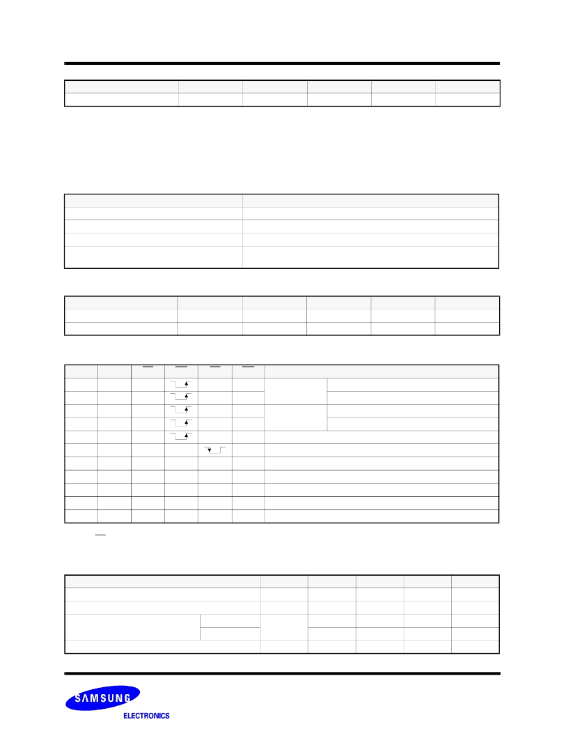
CAPACITANCE
(
T
A
=25
°
C, V
CC
=3.3V, f=1.0MHz)
NOTE
: Capacitance is periodically sampled and not 100% tested.
MODE SELECTION
Item
Symbol
Test Condition
Min
Max
Unit
Input/Output Capacitance
C
I/O
V
IL
=0V
-
10
pF
Input Capacitance
C
IN
V
IN
=0V
-
10
pF
VALID BLOCK
NOTE
:
1. The K9E2G08U0M may include invalid blocks when first shipped. Additional invalid blocks may develop while being used. The number of valid blocks
is presented with both cases of invalid blocks considered. Invalid blocks are defined as blocks that contain one or more bad bits. Do not erase or
program factory-marked bad blocks. Refer to the attached technical notes for a appropriate management of invalid blocks.
2. The 1st block, which is placed on 00h block address, is fully guaranteed to be a valid block, does not require Error Correction up to 1K Program/Erase
cycles.
3. Minimum 2,013 valid blocks are guaranteed for each contiguous 256Mb memory space.
Parameter
Symbol
Min
Typ.
Max
Unit
Valid Block Number
N
VB
16,104
-
16,384
Blocks
AC TEST CONDITION
(K9E2G08U0M-XCB0 :TA=0 to 70
°
C, K9E2G08U0M-XIB0:TA=-40 to 85
°
C)
Parameter
Value
Input Pulse Levels
0.4V to 2.4V
Input Rise and Fall Times
5ns
Input and Output Timing Levels
1.5V
Output Load
VccQ=3.0V+/-10% : 1 TTL GATE and CL= 50pF
VccQ=3.3V+/-10% : 1 TTL GATE and CL=100pF
NOTE
: 1. X can be V
IL
or V
IH.
2. WP should be biased to CMOS high or CMOS low for standby.
CLE
ALE
CE
WE
RE
WP
Mode
H
L
L
H
X
Read Mode
Command Input
L
H
L
H
X
Address Input (4 clocks)
H
L
L
H
H
Write Mode
Command Input
L
H
L
H
H
Address Input (4 clocks)
L
L
L
H
H
Data Input
L
L
L
H
X
Data Output
L
L
L
H
H
X
During Read (Busy)
X
X
X
X
X
H
During Program (Busy)
X
X
X
X
X
H
During Erase (Busy)
X
X
(1)
X
X
X
L
Write Protect
X
X
H
X
X
0V/V
CC
(2)
Stand-by
Program / Erase Characteristics
Parameter
Symbol
Min
Typ
Max
Unit
Program Time
t
PROG
(1)
-
200
500
μ
s
Dummy Busy Time for Multi Plane Program
t
DBSY
1
10
μ
s
Number of Partial Program Cycles
in the Same Page
Main Array
Nop
-
-
1
cycle
Spare Array
-
-
2
cycle
Block Erase Time
t
BERS
-
2
3
ms
NOTE :
1.Typical Program time is defined as the time within which more than 50% of the whole pages are programmed at Vcc of 3.3V and 25’c
相關PDF資料 |
PDF描述 |
|---|---|
| K9E2G08U0M-P | 256M x 8 Bits NAND Flash Memory |
| K9F1208D0A | 64M x 8 Bit , 32M x 16 Bit NAND Flash Memory |
| K9F1208D0A-P | TV 128C 128#22D PIN RECP |
| K9F1208D0A-Y | TV 128C 128#22D PIN RECP |
| K9F1216D0A | 64M x 8 Bit , 32M x 16 Bit NAND Flash Memory |
相關代理商/技術參數 |
參數描述 |
|---|---|
| K9E2G08U0M-P | 制造商:SAMSUNG 制造商全稱:Samsung semiconductor 功能描述:256M x 8 Bits NAND Flash Memory |
| K9E2G08U0M-V | 制造商:SAMSUNG 制造商全稱:Samsung semiconductor 功能描述:256M x 8 Bits NAND Flash Memory |
| K9E2G08U0M-Y | 制造商:SAMSUNG 制造商全稱:Samsung semiconductor 功能描述:256M x 8 Bits NAND Flash Memory |
| K9F1208B0B | 制造商:SAMSUNG 制造商全稱:Samsung semiconductor 功能描述:FLASH MEMORY |
| K9F1208B0C | 制造商:SAMSUNG 制造商全稱:Samsung semiconductor 功能描述:64M x 8 Bits NAND Flash Memory |
發(fā)布緊急采購,3分鐘左右您將得到回復。