- 您現(xiàn)在的位置:買賣IC網(wǎng) > PDF目錄373089 > K9S6408V0A-SSB0 (SAMSUNG SEMICONDUCTOR CO. LTD.) 8M x 8 Bit SmartMediaTM Card PDF資料下載
參數(shù)資料
| 型號: | K9S6408V0A-SSB0 |
| 廠商: | SAMSUNG SEMICONDUCTOR CO. LTD. |
| 英文描述: | 8M x 8 Bit SmartMediaTM Card |
| 中文描述: | 8米× 8位SmartMediaTM卡 |
| 文件頁數(shù): | 2/26頁 |
| 文件大小: | 348K |
| 代理商: | K9S6408V0A-SSB0 |
第1頁當(dāng)前第2頁第3頁第4頁第5頁第6頁第7頁第8頁第9頁第10頁第11頁第12頁第13頁第14頁第15頁第16頁第17頁第18頁第19頁第20頁第21頁第22頁第23頁第24頁第25頁第26頁
K9S6408V0A-SSB0
SmartMedia
TM
2
8M x 8 Bit SmartMedia
TM
Card
The K9S6408V0A is a 8M(8,388,608)x8bit NAND Flash Mem-
ory with a spare 256K(262,144)x8bit. Its NAND cell provides the
most cost-effective solution for the solid state mass storage
market. A program operation programs the 528-byte page in
typically 200
μ
s and an erase operation can be performed in typ-
ically 2ms on an 8K-byte block. Data in the page can be read
out at 50ns cycle time per byte. The I/O pins serve as the ports
for address and data input/output as well as command inputs.
The on-chip write controller automates all program and erase
functions including pulse repetition, where required, and inter-
nal verify and margining of data. Even the write-intensive sys-
tems can take advantage of the K9S6408V0A
′
s extended
reliability of 1,000,000 program/erase cycles by providing
ECC(Error Correcting Code) with real time mapping-out algo-
rithm.
The K9S6408V0A is an optimum solution for large nonvolatile
storage applications such as solid state file storage, digital
voice recorder, digital still camera and other portable applica-
tions requiring non-volatility.
GENERAL DESCRIPTION
FEATURES
Single 2.7V~3.6V Supply
Organization
- Memory Cell Array : (8M + 256K)bit x 8bit
- Data Register : (512 + 16)bit x8bit
Automatic Program and Erase
- Page Program : (512 + 16)Byte
- Block Erase : (8K + 256)Byte
528-Byte Page Read Operation
- Random Access : 7
μ
s(Max.)
- Serial Page Access : 50ns(Min.)
Fast Write Cycle Time
- Program Time : 200
μ
s(Typ.)
- Block Erase Time : 2ms(Typ.)
Command/Address/Data Multiplexed I/O port
Hardware Data Protection
- Program/Erase Lockout During Power Transitions
Reliable CMOS Floating-Gate Technology
- Endurance : 1Million Program/Erase Cycles
- Data Retention : 10 years
Command Register Operation
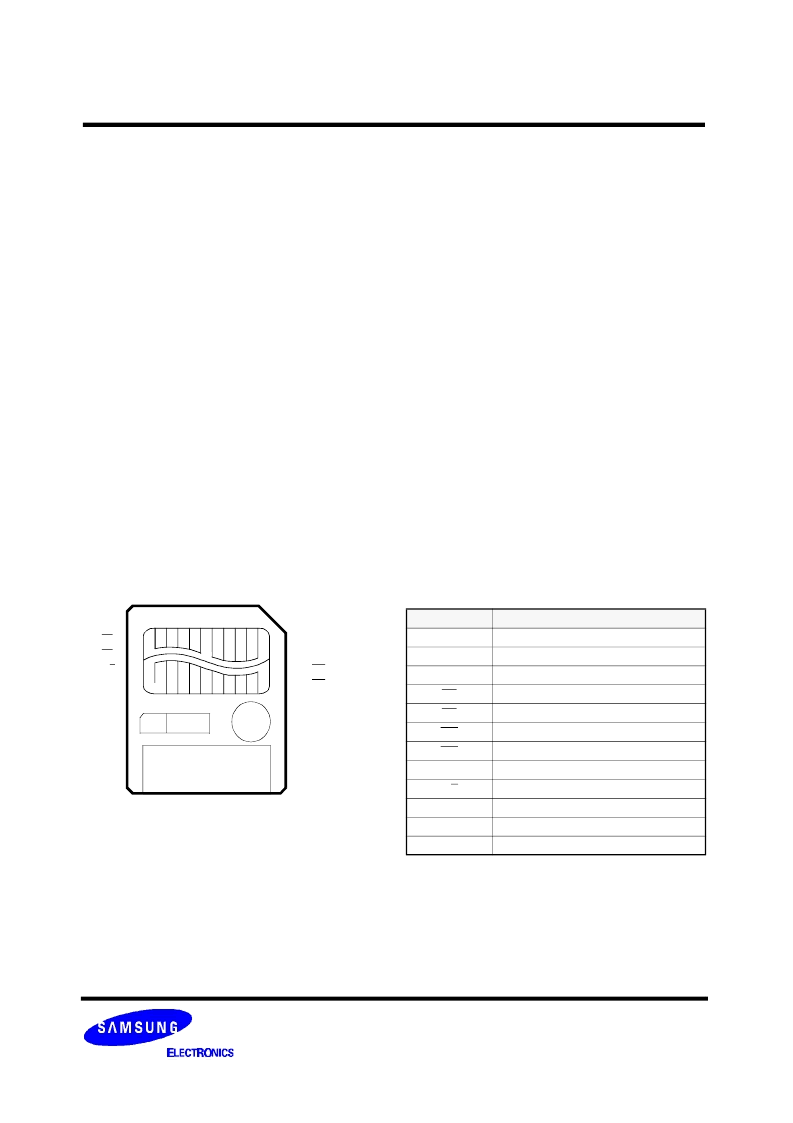
22 pad SmarMedia
TM
(SSFDC)
SmartMedia
TM
CARD(SSFDC)
NOTE
: Connect all V
CC
and V
SS
pins of each device to power supply outputs.
Do not leave V
CC
or V
SS
disconnected.
Pin Name
Pin Function
I/O0 ~ I/O7
Data Input/Outputs
CLE
Command Latch Enable
ALE
Address Latch Enable
CE
Chip Enable
RE
Read Enable
WE
Write Enable
WP
Write Protect
GND
Ground
R/B
Ready/Busy output
V
CC
Power(2.7V~3.6V)
V
SS
Ground
N.C
No Connection
PIN DESCRIPTION
12
22
11
1
12
13
14
15
16
17
18
19
20
21
22
V
CC
I/O
4
I/O
5
I/O
6
I/O
7
V
CC
GND
R/B
RE
CE
V
CC
11
10
9
8
7
6
5
4
3
2
1
V
SS
V
SS
I/O
3
I/O
2
I/O
1
I/O
0
WP
WE
ALE
CLE
V
SS
22 PAD SmartMedia
TM
3V 8MB
相關(guān)PDF資料 |
PDF描述 |
|---|---|
| KA-3020 | 3x2mm SINGLE COLOR SURFACE MOUNT LED LAMPS |
| KA-3020EC | 3x2mm SINGLE COLOR SURFACE MOUNT LED LAMPS |
| KA-3020IT | 3x2mm SINGLE COLOR SURFACE MOUNT LED LAMPS |
| KA-3020SGC | 3x2mm SINGLE COLOR SURFACE MOUNT LED LAMPS |
| KA-3020SGT | 3x2mm SINGLE COLOR SURFACE MOUNT LED LAMPS |
相關(guān)代理商/技術(shù)參數(shù) |
參數(shù)描述 |
|---|---|
| K9S6408V0B | 制造商:SAMSUNG 制造商全稱:Samsung semiconductor 功能描述:SmartMedia CARD |
| K9S6408V0C | 制造商:SAMSUNG 制造商全稱:Samsung semiconductor 功能描述:SmartMedia CARD |
| K9T1G08U0M | 制造商:SAMSUNG 制造商全稱:Samsung semiconductor 功能描述:128M x 8 Bits NAND Flash Memory |
| K9T1G08U0M-YIB0000 | 制造商:Samsung Semiconductor 功能描述:1GB SLC SINGLE (S/B X8 TSOP1 - Trays |
| K9VGMV | 制造商:Micro-Star International 功能描述:- Bulk |
發(fā)布緊急采購,3分鐘左右您將得到回復(fù)。