- 您現(xiàn)在的位置:買賣IC網(wǎng) > PDF目錄373127 > KFH4G16D2M-DIB6 (SAMSUNG SEMICONDUCTOR CO. LTD.) FLASH MEMORY(54MHz) PDF資料下載
參數(shù)資料
| 型號(hào): | KFH4G16D2M-DIB6 |
| 廠商: | SAMSUNG SEMICONDUCTOR CO. LTD. |
| 英文描述: | FLASH MEMORY(54MHz) |
| 中文描述: | 閃存(54MHz之間) |
| 文件頁(yè)數(shù): | 78/125頁(yè) |
| 文件大小: | 1657K |
| 代理商: | KFH4G16D2M-DIB6 |
第1頁(yè)第2頁(yè)第3頁(yè)第4頁(yè)第5頁(yè)第6頁(yè)第7頁(yè)第8頁(yè)第9頁(yè)第10頁(yè)第11頁(yè)第12頁(yè)第13頁(yè)第14頁(yè)第15頁(yè)第16頁(yè)第17頁(yè)第18頁(yè)第19頁(yè)第20頁(yè)第21頁(yè)第22頁(yè)第23頁(yè)第24頁(yè)第25頁(yè)第26頁(yè)第27頁(yè)第28頁(yè)第29頁(yè)第30頁(yè)第31頁(yè)第32頁(yè)第33頁(yè)第34頁(yè)第35頁(yè)第36頁(yè)第37頁(yè)第38頁(yè)第39頁(yè)第40頁(yè)第41頁(yè)第42頁(yè)第43頁(yè)第44頁(yè)第45頁(yè)第46頁(yè)第47頁(yè)第48頁(yè)第49頁(yè)第50頁(yè)第51頁(yè)第52頁(yè)第53頁(yè)第54頁(yè)第55頁(yè)第56頁(yè)第57頁(yè)第58頁(yè)第59頁(yè)第60頁(yè)第61頁(yè)第62頁(yè)第63頁(yè)第64頁(yè)第65頁(yè)第66頁(yè)第67頁(yè)第68頁(yè)第69頁(yè)第70頁(yè)第71頁(yè)第72頁(yè)第73頁(yè)第74頁(yè)第75頁(yè)第76頁(yè)第77頁(yè)當(dāng)前第78頁(yè)第79頁(yè)第80頁(yè)第81頁(yè)第82頁(yè)第83頁(yè)第84頁(yè)第85頁(yè)第86頁(yè)第87頁(yè)第88頁(yè)第89頁(yè)第90頁(yè)第91頁(yè)第92頁(yè)第93頁(yè)第94頁(yè)第95頁(yè)第96頁(yè)第97頁(yè)第98頁(yè)第99頁(yè)第100頁(yè)第101頁(yè)第102頁(yè)第103頁(yè)第104頁(yè)第105頁(yè)第106頁(yè)第107頁(yè)第108頁(yè)第109頁(yè)第110頁(yè)第111頁(yè)第112頁(yè)第113頁(yè)第114頁(yè)第115頁(yè)第116頁(yè)第117頁(yè)第118頁(yè)第119頁(yè)第120頁(yè)第121頁(yè)第122頁(yè)第123頁(yè)第124頁(yè)第125頁(yè)
OneNAND1G(KFG1G16Q2M-DEB5)
FLASH MEMORY
78
OneNAND2G(KFH2G16Q2M-DEB5)
OneNAND4G(KFW4G16Q2M-DEB5)
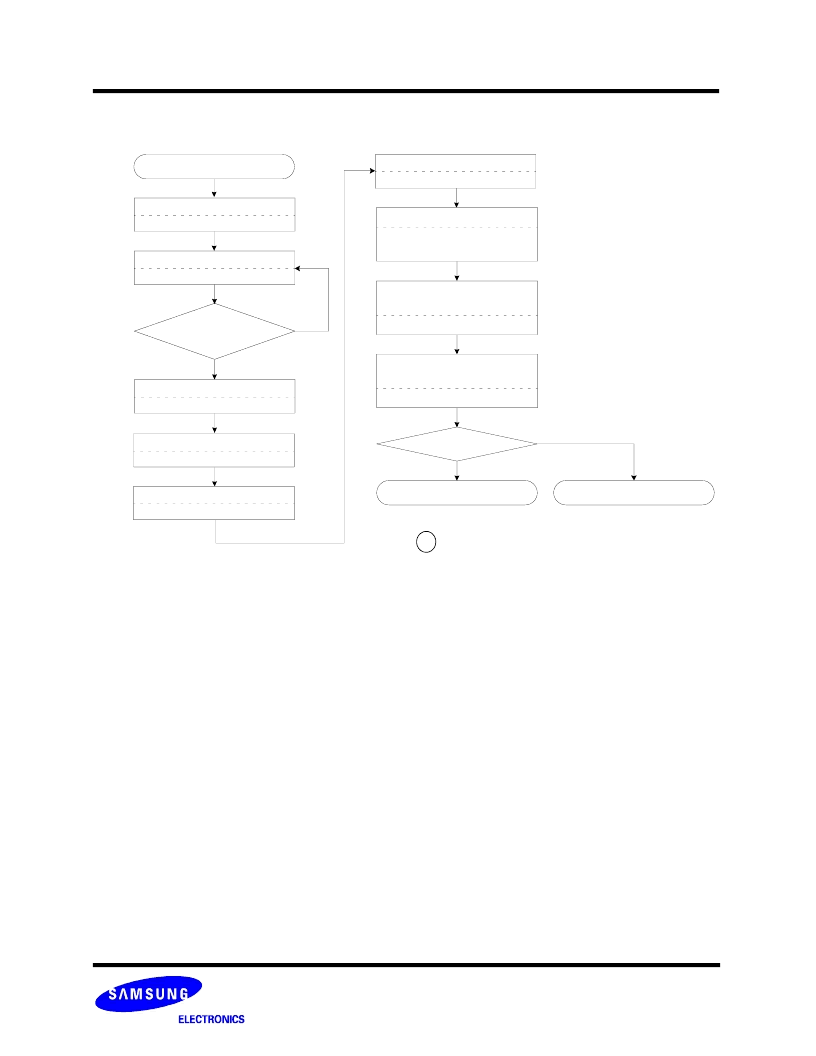
Program Operation Flow Diagram
During the execution of the Internal Program Routine, the host is not required to provide any further controls or
timings. Furthermore, all commands, except a Reset command, will be ignored. A reset during a program operation will cause data
corruption at the corresponding location.
If a program error is detected at the completion of the Internal Program Routine, map out the block, including the page in error, and
copy the target data to another block. An error is signaled if DQ10 = "1" of Controller Status Register(F240h) .
Data input from the Host to the DataRAM can be done at any time during the Internal Program Routine after "Start" but before the
"Write Program Command" is written.
Start
Data Input
Completed
Write ’DFS*, FBA’ of Flash
Add: F100h DQ=DFS, FBA
Write ’FPA, FSA’ of Flash
Add: F107h DQ=FPA, FSA
Select DataRAM for DDP
1)
Add: F101h DQ=DBS*
Write Data into DataRAM
2)
ADD: DP DQ=Data-in
Program completed
Write ’Program’ Command
Add: F220h
DQ=0080h or 001Ah
Wait for INT register
low to high transition
Add: F241h DQ[15]=INT
Read Controller
Status Register
Add: F240h DQ[10]=Error
DQ[10]=0
Program Error
YES
NO
NO
YES
* DBS, DFS is for DDP
: If program operation results in an error, map out
the block including the page in error and copy the
target data to another block.
*
Note 1) This must happen before data input
2) Data input could be done anywhere between "Start" and "Write Program Command".
Write 0 to interrupt register
Add: F241h DQ=0000h
Write ’BSA, BSC’ of DataRAM
Add: F200h DQ=BSA, BSC
相關(guān)PDF資料 |
PDF描述 |
|---|---|
| KFH4G16D2M-DID5 | FLASH MEMORY(54MHz) |
| KFH4G16D2M-DID6 | FLASH MEMORY(54MHz) |
| KFH4G16Q2M-DED5 | FLASH MEMORY(54MHz) |
| KFH4G16Q2M-DED6 | FLASH MEMORY(54MHz) |
| KFH4G16Q2M-DIB6 | FLASH MEMORY(54MHz) |
相關(guān)代理商/技術(shù)參數(shù) |
參數(shù)描述 |
|---|---|
| KFH4G16D2M-DID5 | 制造商:SAMSUNG 制造商全稱:Samsung semiconductor 功能描述:FLASH MEMORY(54MHz) |
| KFH4G16D2M-DID6 | 制造商:SAMSUNG 制造商全稱:Samsung semiconductor 功能描述:FLASH MEMORY(54MHz) |
| KFH4G16Q2M-DEB5 | 制造商:SAMSUNG 制造商全稱:Samsung semiconductor 功能描述:FLASH MEMORY(54MHz) |
| KFH4G16Q2M-DEB6 | 制造商:SAMSUNG 制造商全稱:Samsung semiconductor 功能描述:FLASH MEMORY(54MHz) |
| KFH4G16Q2M-DEB8000 | 制造商:Samsung Semiconductor 功能描述:4GNOFLASHDX1663 FBGA (10X13) - Bulk |
發(fā)布緊急采購(gòu),3分鐘左右您將得到回復(fù)。