- 您現(xiàn)在的位置:買賣IC網(wǎng) > PDF目錄373129 > KFW1G16Q2M-DEB5 (SAMSUNG SEMICONDUCTOR CO. LTD.) FLASH MEMORY(54MHz) PDF資料下載
參數(shù)資料
| 型號(hào): | KFW1G16Q2M-DEB5 |
| 廠商: | SAMSUNG SEMICONDUCTOR CO. LTD. |
| 英文描述: | FLASH MEMORY(54MHz) |
| 中文描述: | 閃存(54MHz之間) |
| 文件頁數(shù): | 15/125頁 |
| 文件大?。?/td> | 1657K |
| 代理商: | KFW1G16Q2M-DEB5 |
第1頁第2頁第3頁第4頁第5頁第6頁第7頁第8頁第9頁第10頁第11頁第12頁第13頁第14頁當(dāng)前第15頁第16頁第17頁第18頁第19頁第20頁第21頁第22頁第23頁第24頁第25頁第26頁第27頁第28頁第29頁第30頁第31頁第32頁第33頁第34頁第35頁第36頁第37頁第38頁第39頁第40頁第41頁第42頁第43頁第44頁第45頁第46頁第47頁第48頁第49頁第50頁第51頁第52頁第53頁第54頁第55頁第56頁第57頁第58頁第59頁第60頁第61頁第62頁第63頁第64頁第65頁第66頁第67頁第68頁第69頁第70頁第71頁第72頁第73頁第74頁第75頁第76頁第77頁第78頁第79頁第80頁第81頁第82頁第83頁第84頁第85頁第86頁第87頁第88頁第89頁第90頁第91頁第92頁第93頁第94頁第95頁第96頁第97頁第98頁第99頁第100頁第101頁第102頁第103頁第104頁第105頁第106頁第107頁第108頁第109頁第110頁第111頁第112頁第113頁第114頁第115頁第116頁第117頁第118頁第119頁第120頁第121頁第122頁第123頁第124頁第125頁
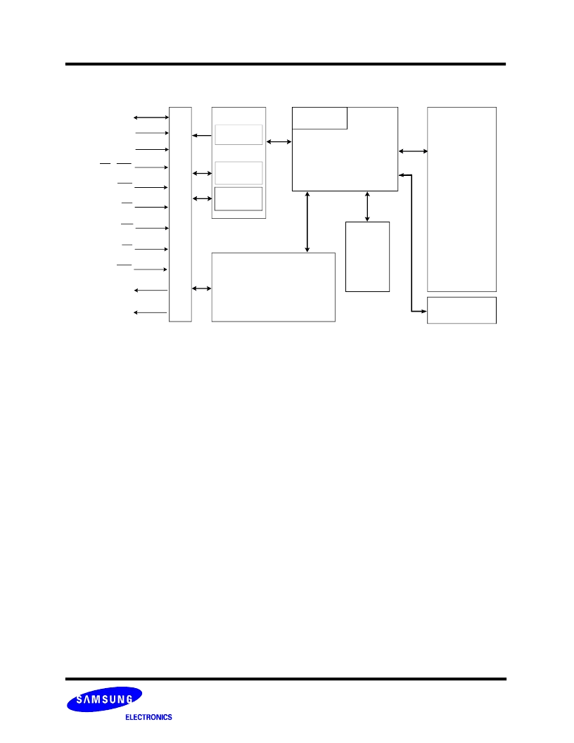
OneNAND1G(KFG1G16Q2M-DEB5)
FLASH MEMORY
15
OneNAND2G(KFH2G16Q2M-DEB5)
OneNAND4G(KFW4G16Q2M-DEB5)
BootRAM
H
CLK
OE
WE
RP
AVD
StateMachine
Bootloader
Internal Registers
(Address/Command/Configuration
/Status Registers)
Error
Correction
Logic
INT
DataRAM0
BufferRAM
NAND Flash
Array
OTP
(One Block)
RDY
A15~A0
DQ15~DQ0
2.6 Memory Array Organization
The OneNAND architecture integrates several memory areas on a single chip.
2.6.1 Internal (NAND Array) Memory Organization
The on-chip internal memory is a single-level-cell (SLC) NAND array used for data storage and code. The internal memory is divided
into a main area and a spare area.
Main Area
The main area is the primary memory array. This main area is divided into Blocks of 64 Pages. Within a Block, each Page is 2KB and
is comprised of 4 Sectors. Within a Page, each Sector is 512B and is comprised of 256 Words.
Spare Area
The spare area is used for invalid block information and ECC storage. Spare area of internal memory is associated with correspond-
ing main area of internal memory. Within a Block, each Page has four 16B Sectors of spare area. Each spare area Sector is 8 words.
DataRAM1
CE2
CE / CE1
2.5 Block Diagram
相關(guān)PDF資料 |
PDF描述 |
|---|---|
| KFG1G16U2M-DEB | FLASH MEMORY |
| KFH1G16U2M-DEB | FLASH MEMORY |
| KFG1G16Q2M-DEB6 | FLASH MEMORY(66MHz) |
| KFW4G16Q2M-DED6 | FLASH MEMORY(66MHz) |
| KFW4G16Q2M | FLASH MEMORY(66MHz) |
相關(guān)代理商/技術(shù)參數(shù) |
參數(shù)描述 |
|---|---|
| KFW1G16Q2M-DEB6 | 制造商:SAMSUNG 制造商全稱:Samsung semiconductor 功能描述:FLASH MEMORY(66MHz) |
| KFW1G16Q2M-DED5 | 制造商:SAMSUNG 制造商全稱:Samsung semiconductor 功能描述:FLASH MEMORY(54MHz) |
| KFW1G16Q2M-DED6 | 制造商:SAMSUNG 制造商全稱:Samsung semiconductor 功能描述:FLASH MEMORY(66MHz) |
| KFW1G16Q2M-DIB5 | 制造商:SAMSUNG 制造商全稱:Samsung semiconductor 功能描述:FLASH MEMORY(54MHz) |
| KFW1G16Q2M-DIB6 | 制造商:SAMSUNG 制造商全稱:Samsung semiconductor 功能描述:FLASH MEMORY(54MHz) |
發(fā)布緊急采購(gòu),3分鐘左右您將得到回復(fù)。