- 您現(xiàn)在的位置:買賣IC網(wǎng) > PDF目錄373180 > KS88P8224 (SAMSUNG SEMICONDUCTOR CO. LTD.) 8-Bit CMOS Microcontroller(8位 CMOS 微控制器) PDF資料下載
參數(shù)資料
| 型號: | KS88P8224 |
| 廠商: | SAMSUNG SEMICONDUCTOR CO. LTD. |
| 英文描述: | 8-Bit CMOS Microcontroller(8位 CMOS 微控制器) |
| 中文描述: | 8位CMOS微控制器(8位的CMOS微控制器) |
| 文件頁數(shù): | 7/7頁 |
| 文件大小: | 65K |
| 代理商: | KS88P8224 |
KS88C8216/C8224/P8224/C8316/C8324/P8324 MICROCONTROLLERS
PRODUCT OVERVIEW
1–7
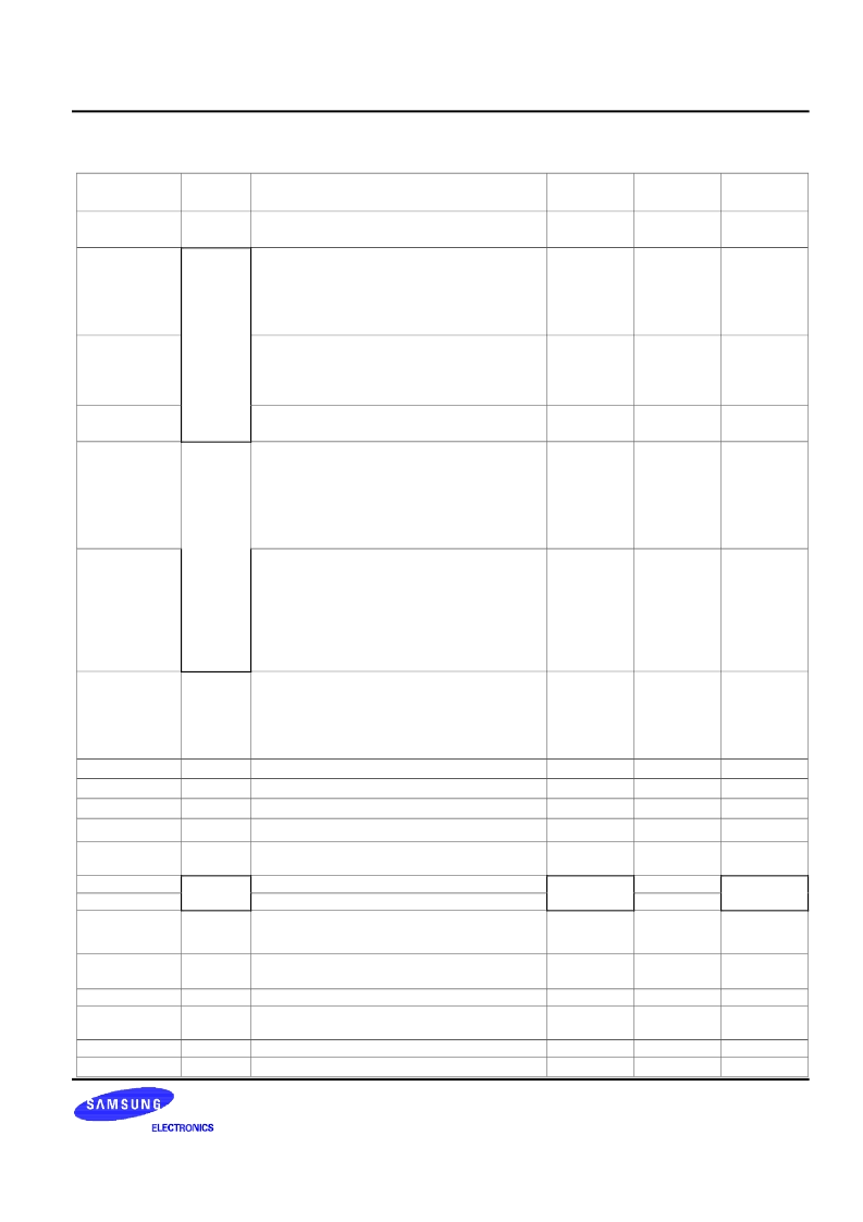
Table 1–1. KS88C8316/C8324 Pin Descriptions
Pin Name
Pin
Type
I/O
Pin Description
Circuit
Type
3
Pin
Numbers
11–12, 35,
38–42
14–15
Share
Pins
P0.0–P0.7
General I/O port (8-bit), configurable for
digital input or push-pull output.
General I/O port (2-bit), configurable for
digital input or n-channel open-drain output.
P1.0–P1.1 can withstand up to 6-volt loads.
Multiplexed for alternative use as external
interrupt inputs INT0–INT1.
General I/O port (4-bit), configurable for
digital input or n-channel open-drain output.
P1.2–P1.5 can withstand up to 6-volt loads.
High current port (10mA).
General I/O port (2-bit), configurable for
digital input or push-pull output.
General I/O port (6-bit). I/O mode or n-
channel open-drain, push-pull output mode
is software configurable. Pins can withstand
up to 5-volt loads.
P2.2: OTP serial clock pin
P2.3: OTP serial data pin
General I/O port (2-bit). I/O mode or n-
channel open-drain, push-pull output mode
is software configurable. Pins can withstand
up to 5-volt loads.
Each pin has an alternative function.
P2.5: PWM0 (14-bit PWM output)
P2.7: OSDHT (Halftone signal output)
General I/O port (2 bits), configurable for
digital input or n-channel open-drain output.
P3.0–P3.1 can withstand up to 5-volt loads.
Multiplexed for alternative use as external
interrupt inputs ADC0–ADC1.
Output pin for 14-bit PWM0 circuit
Analog inputs for 4-bit A/D converter
External interrupt input pins
Halftone control signal output for OSD
Digital blue, green, red, and video blank
signal outputs for OSD
H-sync input for OSD
V-sync input for OSD
L-C oscillator pins for OSD clock frequency
generation
P1.0–P1.1
I/O
7
INT0–INT1
P1.2–P1.5
5
16–19
P1.6–P1.7
3
20, 8
P2.0–P2.4,
P2.6
I/O
2
2–7
P2.5, P2.7
2
1, 21
PWM0
OSDHT
P3.0–P3.1
I/O
6
9–10
ADC0
ADC1
PWM0
ADC0–ADC1
INT0–INT1
OSDHT
Vblue, Vgreen
Vred, Vblank
H-sync
V-sync
OSCIN,
OSCOUT
TEST
O
I
I
O
O
2
6
7
2
4
1
P2.5
9,10
14,15
21
22–25
P3.0–P3.1
P1.0–P1.1
P2.7
–
I
8
26
27
–
I, O
–
28,29
–
I
0V
: Normal Operation Mode,
Vdd
: Test Mode and OTP Write Mode
System clock pins
System reset input pin, Factory test mode is
activated when 12V is applied
Power supply pins
Input for capture A module
–
13
–
XIN, XOUT
RESET
I, O
I
–
1
31,32
33
–
–
VDD, VSS
CAPA
–
I
–
8
13
26
–
–
相關(guān)PDF資料 |
PDF描述 |
|---|---|
| KS88C8216 | 8-Bit CMOS Microcontroller(8位 CMOS 微控制器) |
| KS88C8316 | 8-Bit CMOS Microcontroller(8位 CMOS 微控制器) |
| KS88C9408 | 8-Bit CMOS Microcontroller(8位 CMOS 微控制器) |
| KS88P8324 | SAM87 family of 8-bit single-chip CMOS microcontrollers offers a fast and efficient CPU |
| KS8995M | 5 Port 10/100 Switch with PHY |
相關(guān)代理商/技術(shù)參數(shù) |
參數(shù)描述 |
|---|---|
| KS88P8324 | 制造商:SAMSUNG 制造商全稱:Samsung semiconductor 功能描述:SAM87 family of 8-bit single-chip CMOS microcontrollers offers a fast and efficient CPU |
| KS88P8432 | 制造商:SAMSUNG 制造商全稱:Samsung semiconductor 功能描述:SAM87 family of 8-bit single-chip CMOS microcontrollers offers a fast and efficient CPU |
| KS89-04 | 制造商:Kings Electronics 功能描述: |
| KS8905 | 制造商: 功能描述: 制造商:undefined 功能描述: |
| KS-89-05 | 制造商:WINCHESTER 制造商全稱:Winchester Electronics Corporation 功能描述:K-GRIP ADAPTER |
發(fā)布緊急采購,3分鐘左右您將得到回復。