- 您現(xiàn)在的位置:買賣IC網(wǎng) > PDF目錄383232 > L4938NPD (意法半導(dǎo)體) DUAL MULTIFUNCTION VOLTAGE REGULATOR PDF資料下載
參數(shù)資料
| 型號(hào): | L4938NPD |
| 廠商: | 意法半導(dǎo)體 |
| 英文描述: | DUAL MULTIFUNCTION VOLTAGE REGULATOR |
| 中文描述: | 多功能雙電壓調(diào)節(jié)器 |
| 文件頁數(shù): | 5/12頁 |
| 文件大?。?/td> | 93K |
| 代理商: | L4938NPD |
FUNCTIONAL DESCRIPTION
The L4938N is based on the STMicroelectronics
modular voltage regulator approach. Several out-
standing features and auxiliary functions are pro-
videdtomeet therequirementsofsupplyingthemi-
croprocessor systems used in automotiveapplica-
tions.
Furthermorethe deviceis suitablealso in otherap-
plications requiringtwostabilized voltages.
The modular approach allows other features and
functionsto berealized easily whenrequired.
STANDBYREGULATOR
The standby regulator uses an Isolated Collector
Vertical PNP transistor as the regulating element.
This structure allows a very low dropoutvoltage at
currents up to 50mA. The dropout operationof the
standby regulator is maintained down to 2V input
supply voltage. The output voltage is regulatedup
tothetransientinputsupplyvoltageof40V.Thisfea-
ture avoidsfunctionalinterruptions whichcouldbe
generatedby overvoltagepulses.
The typical curve of thestandbyoutputvoltageas a
functionof theinputsupplyvoltageisshowninfig.1.
The current consumption of the device (quiescent
current) is less than 250
μ
A when output 2 is dis-
abled(standbymode). The dropoutvoltageis con-
trolled to reduce the quiescent current peak in the
undervoltage region and to improve the transient
responsein thisregion.
Thequiescentcurrentisshowninfig.2asafunction
of thesupplyinputvoltage2.
OUTPUT2 VOLTAGE
The output2 regulatorusesthe sameoutputstruc-
tureasthestandbyregulator,butratedforanoutput
current of 500mA.
The output2 regulatorworks in trackingmode with
the standby output voltage as a reference voltage
when the output 2 programming pin ADJ is con-
nectedto V
O2
. By connectinga resistordivider R
1
,
R
2
to thepinADJasshowninfig.3, theoutputvolt-
age 2 canbe programmedto the value:
V
O2
=V
O1
(1 + R
1
/R
2
)
The output 2 regulator can be switched off via the
Enableinput.
If a fixed5 regulationis required ADJPin hasto be
connectedto V
02
Pin.
Note :
1 : V
O2
connected toADJ.V
O2
canbe setto highervalues by inserting an external resistor divider.
2 : Foldback characteristic
ELECTRICAL CHARACTERISTICS
(continued)
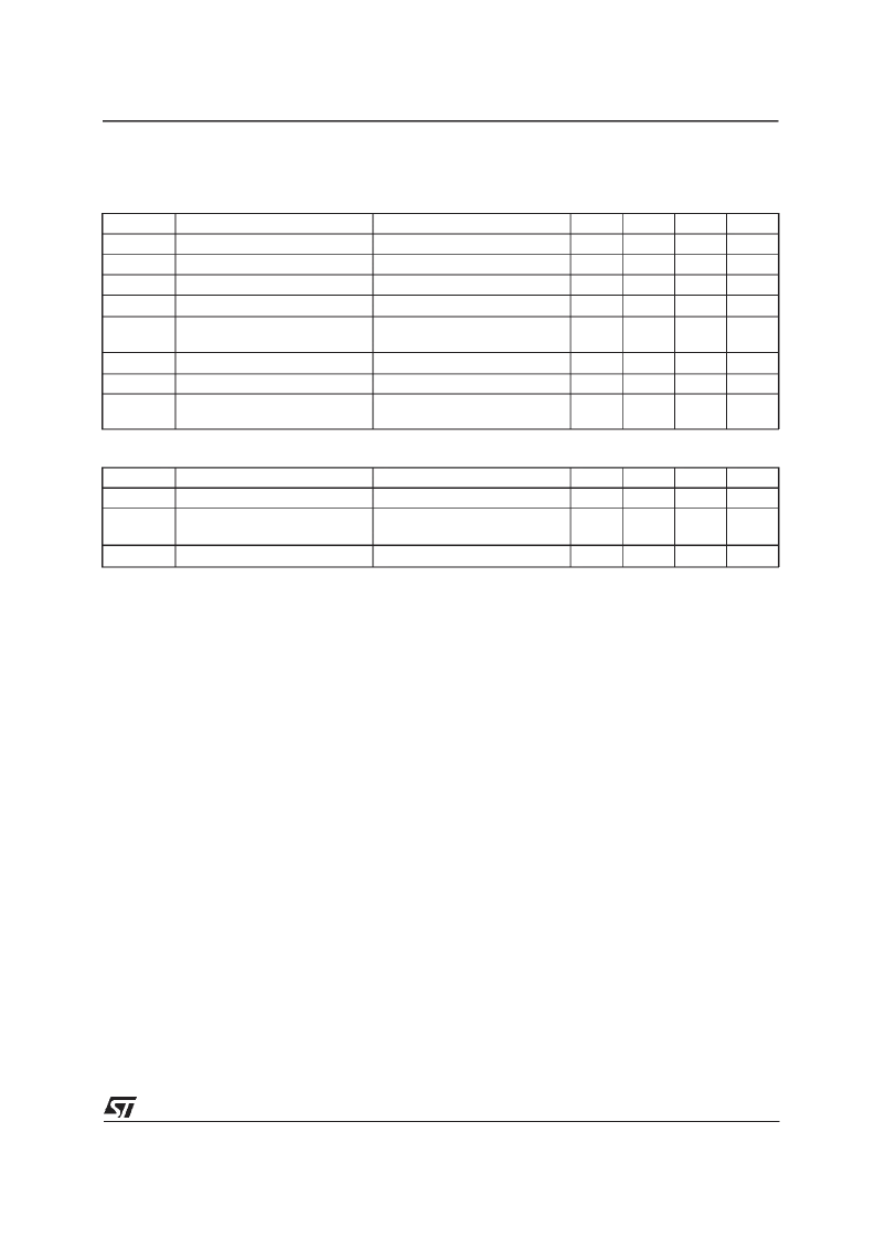
RESET
Symbol
V
Rt
V
Rth
t
RD
t
RR
V
RL
Parameter
Test Conditions
Min.
V
o1
-0.4
50
55
Typ.
4.7
100
100
Max.
V
o1
-0.1
200
180
Unit
V
mV
mV
ResetLow Threshold Voltage
ResetThreshold Hysteresis
ResetPulse Delay
C
T
= 100nF;t
R
> 100
μ
s
C
T
= 100nF
R
RES
= 10K
to V
01
V
S
= 1.5V
V
RES
= 5V
ResetReaction Time
1
10
50
μ
s
V
ResetOutput LOW Voltage
0.4
I
LRES
V
CTh
V
CTh,hyst
ResetOutput HIGH Leakage
Delay Comparator Threshold
Delay Comparator Threshold
Hysteresis
1
μ
A
V
mV
2.0
100
SENSE
V
Slth
V
Slth,hyst
V
SOL
Sense Threshold Voltage
Sense Threshold Hysteresis
Sense OutputLOW Voltage
1.16
40
1.23
100
1.35
200
0.4
V
mV
V
V
SI
= 1,16V;V
S
≥
3V
R
SO
= 10K
to V
01
V
SO
= 5V; V
SI
≥
1.5V
I
LSO
Sense OutputLeakage
1
μ
A
L4938N - L4938ND - L4938NPD
5/12
相關(guān)PDF資料 |
PDF描述 |
|---|---|
| L4938N | DUAL MULTIFUNCTION VOLTAGE REGULATOR |
| L4938ND | DUAL MULTIFUNCTION VOLTAGE REGULATOR |
| L4940V10 | VERY LOW DROP 1.5 A REGULATORS |
| L4940V12 | VERY LOW DROP 1.5 A REGULATORS |
| L4940 | VERY LOW DROP 1.5 A REGULATORS |
相關(guān)代理商/技術(shù)參數(shù) |
參數(shù)描述 |
|---|---|
| L4938NPD013TR | 功能描述:低壓差穩(wěn)壓器 - LDO Dual 5V Very LDO RoHS:否 制造商:Texas Instruments 最大輸入電壓:36 V 輸出電壓:1.4 V to 20.5 V 回動(dòng)電壓(最大值):307 mV 輸出電流:1 A 負(fù)載調(diào)節(jié):0.3 % 輸出端數(shù)量: 輸出類型:Fixed 最大工作溫度:+ 125 C 安裝風(fēng)格:SMD/SMT 封裝 / 箱體:VQFN-20 |
| L493EC | 功能描述:標(biāo)準(zhǔn)LED-通孔 RED WATER CLEAR RoHS:否 制造商:Vishay Semiconductors 照明顏色:Red 光強(qiáng)度:0.7 mcd 波長/色溫:615 nm 顯示角:45 deg 透鏡顏色/類型:Clear, Non-Diffused 正向電流:70 mA 正向電壓:1.83 V to 3.03 V LED 大小:2 mm 系列: 封裝:Tube |
| L-493EC | 制造商:KINGBRIGHT 制造商全稱:Kingbright Corporation 功能描述:T-1 3/4 (5MM) CYLINDRICAL LED LAMPS |
| L-493ED | 制造商:未知廠家 制造商全稱:未知廠家 功能描述:1.0x5.0x10.0mm RECTANGULAR LED LAMP |
| L493GC | 制造商:Kingbright Corporation 功能描述:LED Uni-Color Green 565nm 2-Pin T-1 3/4 |
發(fā)布緊急采購,3分鐘左右您將得到回復(fù)。