- 您現(xiàn)在的位置:買(mǎi)賣(mài)IC網(wǎng) > PDF目錄383237 > L6561 (意法半導(dǎo)體) POWER FACTOR CORRECTOR PDF資料下載
參數(shù)資料
| 型號(hào): | L6561 |
| 廠商: | 意法半導(dǎo)體 |
| 元件分類(lèi): | 基準(zhǔn)電壓源/電流源 |
| 英文描述: | POWER FACTOR CORRECTOR |
| 中文描述: | 功率因數(shù)校正 |
| 文件頁(yè)數(shù): | 4/11頁(yè) |
| 文件大?。?/td> | 115K |
| 代理商: | L6561 |
OVER VOLTAGEPROTECTION OVP
The output voltage is expected to be kept by the
operation of the PFC circuit close to its nominal
value. This is set by the ratio of the two external
resistors R
1
and R
2
(see fig. 2), taking into con-
sideration that the non inverting input of the error
amplifier is biased inside the L6561 at 2.5V.
In steady state conditions,the current through R1
and R2 is:
I
R1sc
=
V
out
2.5
R1
=
I
R2
=
2.5V
R2
and, if the external compensation network is
made only with a capacitor C
comp
, the current
throughC
comp
equalszero.
When the output voltage increases abruptly the
current throughR1 becomes:
I
R1
=
V
outsc
+
V
OUT
2.5
R1
=
I
R1sc
+
I
R1
Since the current through R2 does not change,
I
R1
must flow through the capacitor C
comp
and
enter the error amplifier.
Thiscurrentis monitoredinside theL6561andwhen
reaches about37
μ
A the outputvoltage of themulti-
plier is forcedto decrease,thusreducing theenergy
drawn from the mains. If the current exceeds 40
μ
A,
theOVP protectionis triggered(Dynamic OVP),and
the external power transistor is switched off untilthe
currentfallsapproximatelybelow10
μ
A.
However, if the overvoltage persists, an internal
comparator(Static OVP) confirms the OVP condi-
tion keeping the external power switch turned off
(see fig.1).
Finally, the overvoltage that triggers
functionis:
Vout = R
1
40
μ
A.
Typical values for R
1
, R
2
and C are shown in the
applicationcircuits. Theovervoltagecan be set inde-
pendentlyfrom the averageoutputvoltage.The pre-
cision in setting the overvoltage threshold is 7% of
the OVP
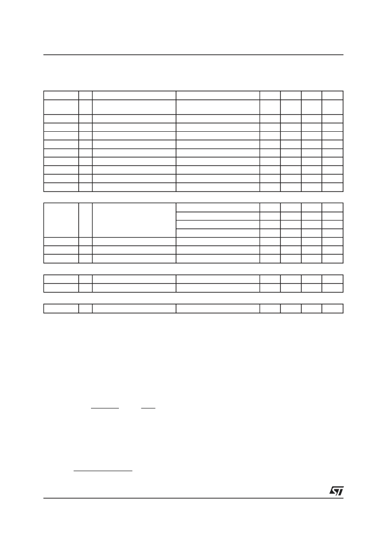
ELECTRICALCHARACTERISTICS
(continued)
ZEROCURRENT DETECTOR
Symbol
V
ZCD
Pin
5
Parameter
Test Condition
Min.
Typ.
2.1
Max.
Unit
V
Input Threshold Voltage
Rising Edge
Hysteresis
Upper Clamp Voltage
Upper Clamp Voltage
Lower Clamp Voltage
Sink Bias Current
Source Current Capability
Sink CurrentCapability
Disable threshold
Restart Current After Disable
(1)
(1)
I
ZCD
= 20
μ
A
I
ZCD
= 3mA
I
ZCD
= –3mA
1V
≤
V
ZCD
≤
4.5V
0.3
4.5
4.7
0.3
0.5
5.1
5.2
0.65
2
0.7
5.9
6.1
1
V
V
V
V
μ
A
mA
mA
mV
μ
A
V
ZCD
V
ZCD
V
ZCD
I
ZCD
I
ZCD
I
ZCD
V
DIS
I
ZCD
5
5
5
5
5
5
5
5
-3
3
150
-100
-10
10
250
-300
200
-200
V
ZCD
< Vdis; V
CC
> V
CCOFF
OUTPUT SECTION
V
GD
7
Dropout Voltage
I
GDsource
= 200mA
I
GDsource
= 20mA
I
GDsink
= 200mA
I
GDsink
= 20mA
C
L
= 1nF
C
L
= 1nF
V
CC
=3.5V V
GD
= 1V
1.2
0.7
2
1
V
V
V
V
ns
ns
mA
1.5
0.3
100
100
-
t
r
t
f
7
7
7
Output Voltage Rise Time
Output Voltage Fall Time
I
GD
Sink Current
40
40
10
I
GD off
5
OUTPUT OVERVOLTAGE SECTION
I
OVP
2
OVP Triggering Current
Static OVP Threshold
35
2.1
40
2.25
45
2.4
μ
A
V
RESTART TIMER
t
START
Start Timer
70
150
400
μ
s
(1) Parameter guaranteedby design,not testedin production.
L6561
4/11
相關(guān)PDF資料 |
PDF描述 |
|---|---|
| L6561D | POWER FACTOR CORRECTOR |
| L6562A | Transition-mode PFC controller |
| L6562AD | Transition-mode PFC controller |
| L6562ADTR | Transition-mode PFC controller |
| L6562AN | Transition-mode PFC controller |
相關(guān)代理商/技術(shù)參數(shù) |
參數(shù)描述 |
|---|---|
| L6561 | 制造商:STMicroelectronics 功能描述:PFC 90UA START + DISABLE 6561 DIP |
| L6561_04 | 制造商:STMICROELECTRONICS 制造商全稱:STMicroelectronics 功能描述:POWER FACTOR CORRECTOR |
| L6561D | 功能描述:功率因數(shù)校正 IC Wide Input Voltage RoHS:否 制造商:Fairchild Semiconductor 開(kāi)關(guān)頻率:300 KHz 最大功率耗散: 最大工作溫度:+ 125 C 安裝風(fēng)格:SMD/SMT 封裝 / 箱體:SOIC-8 封裝:Reel |
| L6561D | 制造商:STMicroelectronics 功能描述:PFC 90UA START + DISABLE SMD 6561 |
| L6561D013TR | 功能描述:功率因數(shù)校正 IC Wide Input Voltage RoHS:否 制造商:Fairchild Semiconductor 開(kāi)關(guān)頻率:300 KHz 最大功率耗散: 最大工作溫度:+ 125 C 安裝風(fēng)格:SMD/SMT 封裝 / 箱體:SOIC-8 封裝:Reel |
發(fā)布緊急采購(gòu),3分鐘左右您將得到回復(fù)。