- 您現(xiàn)在的位置:買賣IC網(wǎng) > PDF目錄383237 > L6563A (意法半導體) ADVANCED TRANSITION-MODE PFC CONTROLLER PDF資料下載
參數(shù)資料
| 型號: | L6563A |
| 廠商: | 意法半導體 |
| 元件分類: | 基準電壓源/電流源 |
| 英文描述: | ADVANCED TRANSITION-MODE PFC CONTROLLER |
| 中文描述: | 先進的轉型模式PFC控制器 |
| 文件頁數(shù): | 19/37頁 |
| 文件大小: | 613K |
| 代理商: | L6563A |
第1頁第2頁第3頁第4頁第5頁第6頁第7頁第8頁第9頁第10頁第11頁第12頁第13頁第14頁第15頁第16頁第17頁第18頁當前第19頁第20頁第21頁第22頁第23頁第24頁第25頁第26頁第27頁第28頁第29頁第30頁第31頁第32頁第33頁第34頁第35頁第36頁第37頁
L6563 - L6563A
Application information
19/37
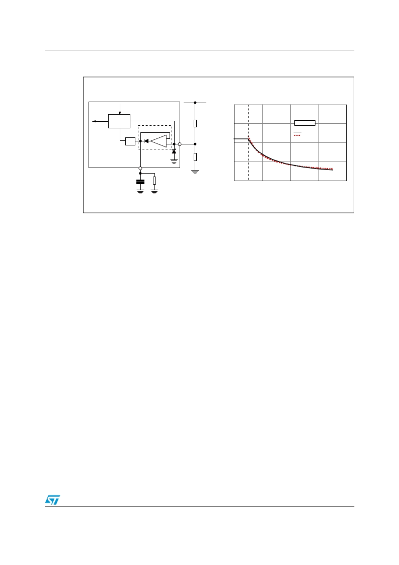
Figure 34. Voltage feedforward: squarer-divider (1/V
2
) block diagram and transfer
characteristic
In this way a change of the line voltage will cause an inversely proportional change of the
half sine amplitude at the output of the multiplier (if the line voltage doubles the amplitude of
the multiplier output will be halved and vice versa) so that the current reference is adapted to
the new operating conditions with (ideally) no need for invoking the slow dynamics of the
error amplifier. Additionally, the loop gain will be constant throughout the input voltage
range, which improves significantly dynamic behavior at low line and simplifies loop design.
Actually, deriving a voltage proportional to the RMS line voltage implies a form of integration,
which has its own time constant. If it is too small the voltage generated will be affected by a
considerable amount of ripple at twice the mains frequency that will cause distortion of the
current reference (resulting in high THD and poor PF); if it is too large there will be a
considerable delay in setting the right amount of feedforward, resulting in excessive
overshoot and undershoot of the pre-regulator's output voltage in response to large line
voltage changes. Clearly a trade-off is required.
The device realizes Voltage Feedforward with a technique that makes use of just two
external parts and that limits the feedforward time constant trade-off issue to only one
direction. A capacitor C
FF
and a resistor R
FF
, both connected from the VFF (pin 5) pin to
ground, complete an internal peak-holding circuit that provides a DC voltage equal to the
peak of the rectified sine wave applied on pin MULT (pin 3). R
FF
provides a means to
discharge C
FF
when the line voltage decreases (see
Figure 34
). In this way, in case of
sudden line voltage rise, C
FF
will be rapidly charged through the low impedance of the
internal diode and no appreciable overshoot will be visible at the pre-regulator's output; in
case of line voltage drop C
FF
will be discharged with the time constant R
FF
·C
FF
, which can
be in the hundred ms to achieve an acceptably low steady-state ripple and have low current
distortion; consequently the output voltage can experience a considerable undershoot, like
in systems with no feedforward compensation.
0
1
2
3
4
0
0.5
1
1.5
2
V
FF
=V
MULT
Vcsx
0.5
V
COMP
=4V
Actual
Ideal
5
MULT
3
R5
Rectified mains
R6
"ideal" diode
current
reference
(Vcsx)
9.5V
VFF
C
FF
R
FF
E/A output
(V
COMP
)
-
+
1/V
2
MULTIPLIER
L6563
L6563A
相關PDF資料 |
PDF描述 |
|---|---|
| L6563ATR | ADVANCED TRANSITION-MODE PFC CONTROLLER |
| L6563 | ADVANCED TRANSITION-MODE PFC CONTROLLER |
| L6563TR | ADVANCED TRANSITION-MODE PFC CONTROLLER |
| L6566A | Multi-mode controller for SMPS with PFC front-end |
| L6566ATR | Multi-mode controller for SMPS with PFC front-end |
相關代理商/技術參數(shù) |
參數(shù)描述 |
|---|---|
| L6563ATR | 功能描述:功率因數(shù)校正 IC Advanced transition mode PFC controller RoHS:否 制造商:Fairchild Semiconductor 開關頻率:300 KHz 最大功率耗散: 最大工作溫度:+ 125 C 安裝風格:SMD/SMT 封裝 / 箱體:SOIC-8 封裝:Reel |
| L6563CYTR | 制造商:ST 功能描述:ADVANCED TRANSITION-MODE PFC CONTROLLER |
| L6563H | 功能描述:功率因數(shù)校正 IC High voltage start Transition-mode PFC RoHS:否 制造商:Fairchild Semiconductor 開關頻率:300 KHz 最大功率耗散: 最大工作溫度:+ 125 C 安裝風格:SMD/SMT 封裝 / 箱體:SOIC-8 封裝:Reel |
| L6563HTR | 功能描述:功率因數(shù)校正 IC 700V 6mA Start-Up Transition-Mode PFC RoHS:否 制造商:Fairchild Semiconductor 開關頻率:300 KHz 最大功率耗散: 最大工作溫度:+ 125 C 安裝風格:SMD/SMT 封裝 / 箱體:SOIC-8 封裝:Reel |
| L6563S | 功能描述:功率因數(shù)校正 IC Transition Mode PFC 5mA 90uA 1.5% Ref RoHS:否 制造商:Fairchild Semiconductor 開關頻率:300 KHz 最大功率耗散: 最大工作溫度:+ 125 C 安裝風格:SMD/SMT 封裝 / 箱體:SOIC-8 封裝:Reel |
發(fā)布緊急采購,3分鐘左右您將得到回復。