- 您現(xiàn)在的位置:買賣IC網(wǎng) > PDF目錄383237 > L6567 (意法半導體) HIGH VOLTAGE DRIVER FOR CFL PDF資料下載
參數(shù)資料
| 型號: | L6567 |
| 廠商: | 意法半導體 |
| 英文描述: | HIGH VOLTAGE DRIVER FOR CFL |
| 中文描述: | 高壓驅動節(jié)能燈 |
| 文件頁數(shù): | 5/15頁 |
| 文件大?。?/td> | 115K |
| 代理商: | L6567 |
5/15
L6567
(*) Before starting the first commutation; when switching 6V is guaranteed.
General operation
The L6567 uses a small amount of current from a supply resistor(s) to start the operation of the IC. Once start
up condition is achieved, the IC turns on the lower MOS transistor of the half bridge which allows the bootstrap
capacitor to charge. Once this is achieved, the oscillator begins to turn on the upper and lower MOS transistors
at high frequency, and immediately ramps down to a preheat frequency. During this stage, the IC preheats the
lamp and after a predetermined time ramps down again until it reaches the final operating frequency. The IC
monitors thecurrent to determine if the circuitisoperating in capacitive mode. If capacitive switching is detected,
the IC increases the output frequency until zero-voltage switching is resumed.
Startup and supply in normaloperation
At start up the L6567 is powered via a resistor connected to the R
HV
pin (pin 13) from the rectified mains. The
current charges the C
S
capacitor connected to the V
S
pin (pin 5). When the V
S
voltage reaches the threshold
V
S LOW1
(max 6V), the low side MOS transistor is turned on while the high side one is kept off. This condition
assures that the bootstrap capacitor is charged. When V
SHIGH1
threshold is reached the oscillator starts, and
the R
HV
pin does not provide anymore the supply current for the IC (see fig.1).
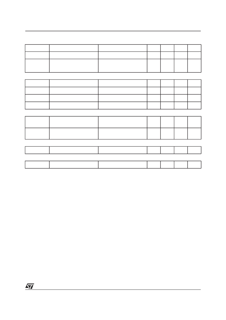
G2
DON
On Delay of G2 Output
1.05
1.4
1.75
μ
s
Ratio between Delay Time +
Conduction Time of G1 and G2
I
RHV
= 1mA; Cl = 5V
Cl = 0V
0.87
0.77
1.15
1.30
LOW SIDE DRIVER SECTION
Ron G2 so
G2 Source Output Resistance
V
S
= 12V,V = 3V
80
190
Ron G2 si
G2 Sink Output Resistance
V
S
= 12V,V = 3V
65
125
Ron G1 so
G1 Source Output Resistance
V
S
= 10V,V = 3V
80
190
Ron G1 si
G1 Sink Output Resistance
V
S
= 10V,V = 3V
65
125
HIGH SIDE DRIVER SECTION
I
FSLK
Leakage Current of FS PIN to
GND
V
FS
= 568V; G1 = L
V
FS
= 568V; G1 = H
5
5
μ
A
μ
A
I
S1 LK
Leakage Current of S1 PIN to
GND
V
S1
= 568V; G1 = L
V
S1
= 568V; G1 = H
5
5
μ
A
μ
A
BOOTSTRAP SECTION
Boot Th
BOOTSTRAP Threshold
V
S
= 10.6V before turn on
5 (*)
V
AVERAGE RESISTOR
R
AVERAGE
Average Resistor
27
38.5
50
k
Symbol
Parameter
Test Condition
Min.
Typ.
Max.
Unit
G1
DON
G1
ON
+
---------------------+
ELECTRICAL CHARACTERISTCS
(Continued)
相關PDF資料 |
PDF描述 |
|---|---|
| L6567D | HIGH VOLTAGE DRIVER FOR CFL |
| L6571B | High Voltage Half Bridge Driver with Oscillator(帶晶振的高電壓半橋驅動器) |
| L6585D | PFC and Ballast Control IC |
| L6585DTR | PFC and Ballast Control IC |
| L6590 | Fully Integrated Power Supply FIPSTM(完全集成電源) |
相關代理商/技術參數(shù) |
參數(shù)描述 |
|---|---|
| L6567D | 制造商:STMicroelectronics 功能描述:CFL DRVR 18V 14SOP - Rail/Tube |
| L6569 | 功能描述:功率驅動器IC Hi-Volt Half Bridge RoHS:否 制造商:Micrel 產(chǎn)品:MOSFET Gate Drivers 類型:Low Cost High or Low Side MOSFET Driver 上升時間: 下降時間: 電源電壓-最大:30 V 電源電壓-最小:2.75 V 電源電流: 最大功率耗散: 最大工作溫度:+ 85 C 安裝風格:SMD/SMT 封裝 / 箱體:SOIC-8 封裝:Tube |
| L6569 | 制造商:STMicroelectronics 功能描述:IC HALF BRIDGE+OSC 6569 DIP8 |
| L6569A | 功能描述:功率驅動器IC Hi-Volt Half Bridge RoHS:否 制造商:Micrel 產(chǎn)品:MOSFET Gate Drivers 類型:Low Cost High or Low Side MOSFET Driver 上升時間: 下降時間: 電源電壓-最大:30 V 電源電壓-最小:2.75 V 電源電流: 最大功率耗散: 最大工作溫度:+ 85 C 安裝風格:SMD/SMT 封裝 / 箱體:SOIC-8 封裝:Tube |
| L6569A | 制造商:STMicroelectronics 功能描述:IC HALF BRIDGE+OSC 6569 DIP8 |
發(fā)布緊急采購,3分鐘左右您將得到回復。