- 您現(xiàn)在的位置:買賣IC網(wǎng) > PDF目錄383238 > L6919CD (意法半導(dǎo)體) 5 BIT PROGRAMMABLE DUAL-PHASE CONTROLLER WITH DYNAMIC VID MANAGEMENT PDF資料下載
參數(shù)資料
| 型號: | L6919CD |
| 廠商: | 意法半導(dǎo)體 |
| 英文描述: | 5 BIT PROGRAMMABLE DUAL-PHASE CONTROLLER WITH DYNAMIC VID MANAGEMENT |
| 中文描述: | 5位可編程雙相與動(dòng)態(tài)VID管理控制器 |
| 文件頁數(shù): | 12/32頁 |
| 文件大小: | 558K |
| 代理商: | L6919CD |
第1頁第2頁第3頁第4頁第5頁第6頁第7頁第8頁第9頁第10頁第11頁當(dāng)前第12頁第13頁第14頁第15頁第16頁第17頁第18頁第19頁第20頁第21頁第22頁第23頁第24頁第25頁第26頁第27頁第28頁第29頁第30頁第31頁第32頁
L6919C
12/32
follow:
Since the current is read in differential mode, also negative current information is kept; this allow the device to
check for dangerous returning current between the two phases assuring the complete equalization between the
phase's currents. From the current information of each phase, information about the total current delivered (I
FB
=I
INFO1
+I
INFO2
) and the average current for each phase (I
AVG
=(I
INFO1
+I
INFO2
)/2 ) is taken. I
INFOX
is then com-
pared to I
AVG
to give the correction to the PWM output in order to equalize the current carried by the two phases.
The transconductance resistor Rg can be designed in order to have current information of 25
μ
A per phase at
full nominal load; the over current intervention threshold is set at 140% of the nominal (I
INFOx
= 35
μ
A). According
to the above relationship, the over current threshold (I
OCPx
) for each phase, which has to be placed at one half
of the total delivered maximum current, results:
Since the device senses the output current across the low-side mosfets (or across a sense resistors in series
with them) the device limits the bottom of the inductor current triangular waveform: an over current is detected
when the current flowing into the sense element is greater than I
OCPx
(I
INFOx
> 35
μ
A).
Introducing now the maximum ON time dependence with the delivered current (where T is the switching period
T=1/f
SW
):
R
---------------------
I
OUT
5.73k
This linear dependence has a value at zero load of 0.80·T and at maximum current of 0.40·T typical and results
in two different behaviors of the device:
1. T
ON
Limited Output Voltage.
This happens when the maximum ON time is reached before the current in each phase reaches I
OCPx
(I
INFOx
< 35
μ
A).
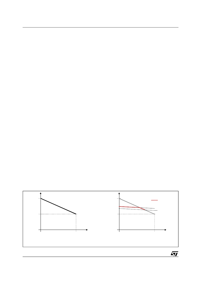
Figure 6a shows the maximum output voltage that the device is able to regulate considering the T
ON
limitation
imposed by the previous relationship. If the desired output characteristic crosses the T
ON
limited maximum output
voltage, the output resulting voltage will start to drop after crossing. In this case, the device doesn't perform con-
stant current limitation but only limits the maximum ON time following the previous relationship. The output volt-
age follows the resulting characteristic (dotted in Figure 6b) until UVP is detected or anyway until I
FB
= 70
μ
A.
Figure 6. T
ON
Limited Operation
I
INFOx
R
I
R
g
----------------------------------------------
=
I
OCPx
R
SENSE
---------------------------
=
Rg
I
R
35
μ
A
------------------------------------------
=
T
ON,MAX
0.80
I
FB
5.73k
(
)
T
–
0.80
Rg
T
0.80 T I
FB
0.40 T I
FB
0
μ
A
=
70
μ
A
=
–
=
=
a) Maximum output Voltage
b) T
ON
Limited Output Voltage
0.80·V
IN
0.40·V
IN
V
OUT
I
OUT
I
OCP
=2·I
OCPx
(I
FB
=70
μ
T
ON
Limited Output
characteristic
0.80·V
IN
0.40·V
IN
V
OUT
I
OUT
I
OCP
=2·I
OCPx
(I
FB
=70
μ
Desired Output
characteristic and
UVP threshold
Resulting Output
characteristic
相關(guān)PDF資料 |
PDF描述 |
|---|---|
| L6919CDTR | CAP 20PF 50V 5% C0G SMD-0805 TR-7-PL SN100 |
| L6920DB | Synchronous rectifier step up converter |
| L6920DBTR | Synchronous rectifier step up converter |
| L6920DTR | 1V HIGH EFFICIENCY SYNCRONOUS STEP UP CONVERTER |
| L6920D | 1V HIGH EFFICIENCY SYNCRONOUS STEP UP CONVERTER |
相關(guān)代理商/技術(shù)參數(shù) |
參數(shù)描述 |
|---|---|
| L6919CDTR | 功能描述:DC/DC 開關(guān)控制器 Prog Dual-Phase Cont RoHS:否 制造商:Texas Instruments 輸入電壓:6 V to 100 V 開關(guān)頻率: 輸出電壓:1.215 V to 80 V 輸出電流:3.5 A 輸出端數(shù)量:1 最大工作溫度:+ 125 C 安裝風(fēng)格: 封裝 / 箱體:CPAK |
| L6919E | 功能描述:DC/DC 開關(guān)控制器 5-Bit Dual Ph Contlr RoHS:否 制造商:Texas Instruments 輸入電壓:6 V to 100 V 開關(guān)頻率: 輸出電壓:1.215 V to 80 V 輸出電流:3.5 A 輸出端數(shù)量:1 最大工作溫度:+ 125 C 安裝風(fēng)格: 封裝 / 箱體:CPAK |
| L6919ETR | 功能描述:DC/DC 開關(guān)控制器 5-Bit Dual Ph Contlr RoHS:否 制造商:Texas Instruments 輸入電壓:6 V to 100 V 開關(guān)頻率: 輸出電壓:1.215 V to 80 V 輸出電流:3.5 A 輸出端數(shù)量:1 最大工作溫度:+ 125 C 安裝風(fēng)格: 封裝 / 箱體:CPAK |
| L-692 | 制造商:RHOMBUS-IND 制造商全稱:Rhombus Industries Inc. 功能描述:Common Mode Inductor |
| L6920 | 制造商:STMICROELECTRONICS 制造商全稱:STMicroelectronics 功能描述:1V HIGH EFFICIENCY SYNCRONOUS STEP UP CONVERTER |
發(fā)布緊急采購,3分鐘左右您將得到回復(fù)。