- 您現(xiàn)在的位置:買賣IC網(wǎng) > PDF目錄39185 > L6997STR (STMICROELECTRONICS) SWITCHING CONTROLLER, PDSO20 PDF資料下載
參數(shù)資料
| 型號(hào): | L6997STR |
| 廠商: | STMICROELECTRONICS |
| 元件分類: | 穩(wěn)壓器 |
| 英文描述: | SWITCHING CONTROLLER, PDSO20 |
| 封裝: | MO-153-AC, TSSOP-20 |
| 文件頁數(shù): | 8/30頁 |
| 文件大?。?/td> | 546K |
| 代理商: | L6997STR |
第1頁第2頁第3頁第4頁第5頁第6頁第7頁當(dāng)前第8頁第9頁第10頁第11頁第12頁第13頁第14頁第15頁第16頁第17頁第18頁第19頁第20頁第21頁第22頁第23頁第24頁第25頁第26頁第27頁第28頁第29頁第30頁

L6997S
16/30
6
STEP BY STEP DESIGN
Application conditions: VIN = 3.3V, ±10% VOUT = 1.25V IOUT = 5A FSW = 270kHz
6.1 Input capacitor.
A pulsed current (with zero average value) flows through the input capacitor of a buck converter. The AC com-
ponent of this current is quite high and dissipates a considerable amount of power on the ESR of the capacitor:
(17)
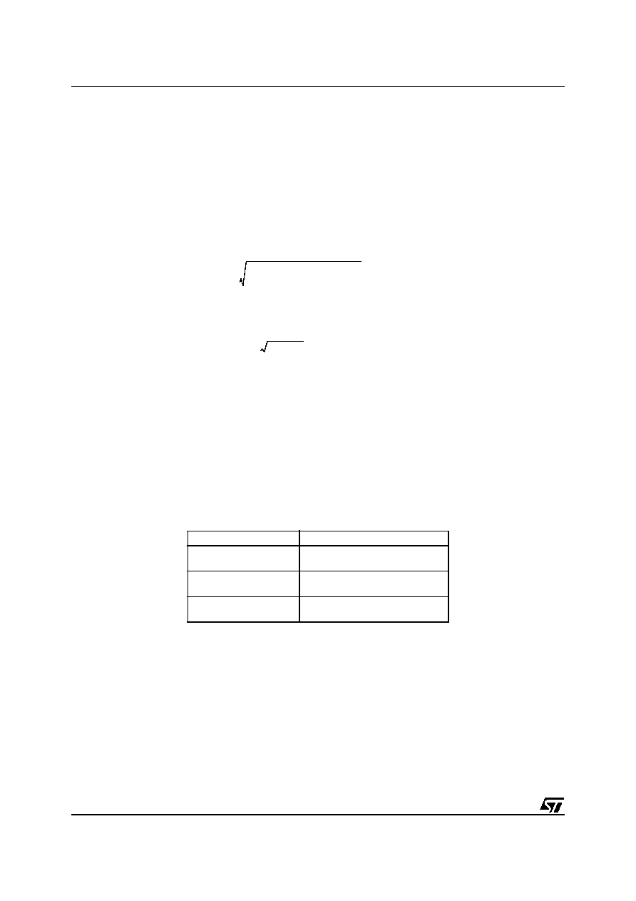
The RMS current, which the capacitor must provide, is given by:
(18)
Where
δ is the duty cycle of the application
Neglecting the last term, the equation reduces to:
(19)
which maximum value corresponds to to
δ = 1/2 and is equal Iout/2
Therefore, in worst case, the input capacitors should be selected with a RMS ripple current rating as high as
half the respective maximum output current.
Electrolytic capacitors are the most used because theyare the cheapest ones and are available with a wide
range of RMS current ratings. The only drawback is that, for a givenripple current rating, they are physically larg-
er than other capacitors. Very good tantalum capacitors are coming available, with very low ESR and small size.
The only problem is that they occasionally can burn if subjected to very high current during the charge. So, it is
better avoid this type of capacitors for the input filter of the device. In fact, they can be subjected to high surge
current when connected to the power supply. If available for the requested capacitance value and voltage rating,
the ceramic capacitors have usually a higher RMS current rating for a given physical dimension (due to the very
low ESR). The drawback is the quite high cost. Possible solutions:
With our parameter from the equation 3 it is found:
Icinrms = 2.42A
6.2 Inductor
To define the inductor, it is necessary to determine firstly the inductance value. Its minimum value is given by:
(20)
where RF =
I/IOUT (basically it is approximately 30%).
10
F
C34Y5U1E106ZTE12 TOKIN
22
F
JMK325BJ226MM
TAIYO-YUDEN
47
F
ECJ4XF0J476Z
PANASONIC
33
F
C3225X5R0J476M
TDK
P
CIN
ESR
CIN
Iout
2
Vin
Vout
–
()
Vin
2
------------------------------------------------
=
Icin
rms
Iout
2 δ 1 δ
–
()
δ
12
------
I
L
()
2
+
=
Icin
rms
Iout
δ 1 δ
–
()
=
Lmin
V
o
Vin
max
V
o
–
()
F
SW
I
out
RF Vin
max
---------------------------------------------------------------
≥
相關(guān)PDF資料 |
PDF描述 |
|---|---|
| L8020G-S08-R | SPECIALTY ANALOG CIRCUIT, PDSO8 |
| L8115G-R16-R | SPECIALTY ANALOG CIRCUIT, PDSO16 |
| L8115-R20-R | SPECIALTY ANALOG CIRCUIT, PDSO20 |
| L8115G-R20-R | SPECIALTY ANALOG CIRCUIT, PDSO20 |
| L8115L-R16-R | SPECIALTY ANALOG CIRCUIT, PDSO16 |
相關(guān)代理商/技術(shù)參數(shù) |
參數(shù)描述 |
|---|---|
| L6998-0 | 制造商:Johanson Manufacturing 功能描述:TUNING ELEMENT |
| L6998-1 | 制造商:Johanson Manufacturing 功能描述:TUNING ELEMENT |
| L6998-5 | 制造商:Johanson Manufacturing 功能描述:TUNING ELEMENT |
| L6998-6 | 制造商:Johanson Manufacturing 功能描述:TUNING ELEMENT |
| L6999 | 制造商:HAMAMATSU 制造商全稱:Hamamatsu Corporation 功能描述:The best light source is supported by the best electrode technology |
發(fā)布緊急采購,3分鐘左右您將得到回復(fù)。