- 您現(xiàn)在的位置:買賣IC網(wǎng) > PDF目錄30713 > LA1135M AM, AUDIO SINGLE CHIP RECEIVER, PDSO20 PDF資料下載
參數(shù)資料
| 型號(hào): | LA1135M |
| 元件分類: | 接收器 |
| 英文描述: | AM, AUDIO SINGLE CHIP RECEIVER, PDSO20 |
| 封裝: | MFP-20 |
| 文件頁數(shù): | 2/20頁 |
| 文件大小: | 294K |
| 代理商: | LA1135M |

LA1135, 1135M
No.1272-10/20
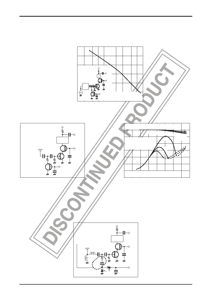
16. Measure against suppression of sensitivity in the presence of an undesired signal of high strength
(Sample application where two PIN diodes are used in the antenna damping circuit)
The LA1135 contains the wide-band AGC circuit (wide-band AGC with pin 2 input) against cross modulation which
occurs because an undesired signal of high strength distorts the FET input. The AGC = ON level depends on the value
of external resistor R3 as shown below.
When a nonlinear element, such as transistor, is used for antenna damping, cross modulation which occurs when the
transistor is turned ON is as shown below.
The dynamic range of the FET input covers up to approximately 110dB
μ of antenna input, but the AGC-ON level must be
set lower because of the bad effect shown above.
Therefore, there are some cases where it is difficult to receive a desired signal of low strength in the presence of an an
undesired signal of high strength. To solve this problem, a sample application circuit where two PIN diodes with good
linearity are used for antenna damping and its cross modulation characteristic are shown below.
Sample Application Circuit where two PIN diodes are used for ANT damping
Cross modulation characteristic which is caused
by the ANT Tr when the
LA1135 wide-band
AGC-ON level (with
pin 2 input) is varied
VDD=8V
Double-
tuning
2
0.047
μF × 2
0.022
μF
22
μ
F
0.022
μ
F
100k
Ω
51
Ω
R3
1
4
– 70
– 30
– 20
– 10
0
– 40
– 50
– 60
10
50
90
70
80
60
100
120
110
130
Undesired input – dB
μ
Output
–
d
B
Desired : 1.0MHz 400Hz 30%mod 74dB
μ
Undesired : 1.4MHz non-mod
Cross modulation which occurs when the
transistor for ANT damping is turned ON
Desired : 1.0MHz 400Hz
non-mod 74dB
μ
Undesired : 1.4MHz 1kHz
80%mod
20
Ω
20
Ω
51
Ω
75
Ω
Wide-band AGC
(pin 2 input)75Ω
pick up R3
51
Ω
VDD = 8V
2
0.022
μF × 2
100
μH
0.022
μF
22
μ
F
0.022
μ
F
0.022
μF
100k
Ω
5Ω
51
Ω
1
4
diode
pin
3.3mH
Equivalent capacitance available
(Capacitance is desirable because
of a slight change in ANT damping
in the band)
(Approximately 3000pF)
Double-
tuning
VDD = 8V
Double-tuning
2
1
2SC536
2SC315
JIS
antd
2SC930
fu
R3
22
μF
51
Ω
50
Ω
80
100
105
95
90
85
110
2
10
57
32
5
7
3
100
Resistor value, R –
Ω
W
.B.AGC-ON
level
–
d
B
μ
Test conditions
ANT input level
at which ANTD is turned ON when
fu = 1.4MHz is inputed at fr = 1MHz
相關(guān)PDF資料 |
PDF描述 |
|---|---|
| LA1137NM | AM, AUDIO SINGLE CHIP RECEIVER, PDSO20 |
| LA1137N | AM, AUDIO SINGLE CHIP RECEIVER, PDIP20 |
| LA1136NM | AM, AUDIO SINGLE CHIP RECEIVER, PDSO24 |
| LA1136N | AM, AUDIO SINGLE CHIP RECEIVER, PDIP24 |
| LA1143 | FM, AUDIO DEMODULATOR, PDIP16 |
相關(guān)代理商/技術(shù)參數(shù) |
參數(shù)描述 |
|---|---|
| LA1136 | 制造商:SANYO 制造商全稱:Sanyo Semicon Device 功能描述:AM Tuners for Car Radios and Home Stereos |
| LA1136M | 制造商:未知廠家 制造商全稱:未知廠家 功能描述: |
| LA1136N | 制造商:SANYO 制造商全稱:Sanyo Semicon Device 功能描述:AM Tuners for Car Radios and Home Stereos |
| LA1136NM | 制造商:SANYO 制造商全稱:Sanyo Semicon Device 功能描述:AM Tuners for Car Radios and Home Stereos |
| LA1137 | 制造商:SANYO 制造商全稱:Sanyo Semicon Device 功能描述:AM Tuners for Car Radios and Home Stereos |
發(fā)布緊急采購,3分鐘左右您將得到回復(fù)。