- 您現(xiàn)在的位置:買賣IC網(wǎng) > PDF目錄30718 > LA4555 2.3 W, 2 CHANNEL, AUDIO AMPLIFIER, PDIP12 PDF資料下載
參數(shù)資料
| 型號: | LA4555 |
| 元件分類: | 音頻/視頻放大 |
| 英文描述: | 2.3 W, 2 CHANNEL, AUDIO AMPLIFIER, PDIP12 |
| 封裝: | DIP-12 |
| 文件頁數(shù): | 5/10頁 |
| 文件大?。?/td> | 364K |
| 代理商: | LA4555 |

LA4555
No.1697–4/10
Continued from preceding page.
C7 (C8) : Output capacitor. The low cutoff frequency is determined by the following formula.
fL : Low cutoff frequency
RL : Load resistance
To make the low frequency response in the bridge amplifier mode identical with that in the stereo mode, the
capacitor value must be doubled.
C9 :
Decoupling capacitor. Used for the ripple filter. Since the rejection effect is saturated at a certain capacitor
value, it is meaningless to increase the capacitor value more than needed. This capacitor, being also used for
the time constant of the muting circuit, affects the starting time.
C10 :
Power source capacitor.
Application Circuits
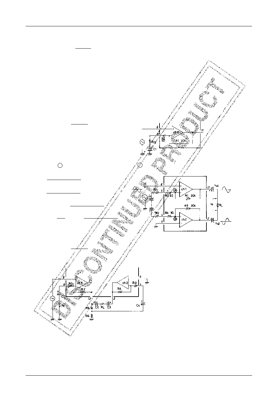
Voltage gain adjust
Stereo mode
The voltage gain is determined by on-chip resistor R1 (R2) and external feedback resistor Rf as follows :
Any voltage gain can be obtained by external
resistor Rf.
Bridge amplifier 1 mode
Since point A is at the same potential as Vi and point B is a virtual GND point,
Assuming R2=R4=50
, R1=R3=20k and Rf1=Rf2, the voltage gain is obtained by :
Bridge amplifier 2 mode
The CH1 is a noninverting amplifer and the CH2 is an inverting amplifier. The total voltage gain, being apparently
higher than that of the CH1 by 6dB, is approximately calculated by the following formula.
VG=20log R2/R1+6 (dB)
To reduce the voltage gain, Rf is connected and the following formula is used.
VG=20log R2/Rf+R1+6 (dB)
fL=
1
2
πC7RL
VG=20 log
[dB]
R1
Rf1+R2
Vo1
≈
Vi
R1
R2+R4+Rf1+Rf2
VG=20 log
[dB]
R1
Rf1+R2
Vo2
≈
Vi
–R3
R2+R4+Rf1+Rf2
VG=20 log
=20log
[dB]
Vo
Vi
R1+R3
R2+R4+Rf1+Rf2
Vo = Vo1 – Vo2 =
Vi
R1+R3
R2+R4+Rf1+Rf2
相關(guān)PDF資料 |
PDF描述 |
|---|---|
| LA4557 | 2.4 W, 2 CHANNEL, AUDIO AMPLIFIER, PDIP12 |
| LA4558 | 2.4 W, 2 CHANNEL, AUDIO AMPLIFIER, PDIP12 |
| LA4571MB | 0.032 W, 2 CHANNEL, AUDIO AMPLIFIER, PDSO20 |
| LA4571MB | 0.032 W, 2 CHANNEL, AUDIO AMPLIFIER, PDSO20 |
| LA4575 | 0.038 W, 2 CHANNEL, AUDIO AMPLIFIER, PDIP16 |
相關(guān)代理商/技術(shù)參數(shù) |
參數(shù)描述 |
|---|---|
| LA4557 | 制造商:Panasonic Industrial Company 功能描述:IC |
| LA4558 | 制造商:Panasonic Industrial Company 功能描述:IC |
| LA4560M | 制造商:未知廠家 制造商全稱:未知廠家 功能描述:Analog IC |
| LA4570 | 制造商:未知廠家 制造商全稱:未知廠家 功能描述:Analog IC |
| LA4570M | 制造商:未知廠家 制造商全稱:未知廠家 功能描述:Analog IC |
發(fā)布緊急采購,3分鐘左右您將得到回復(fù)。