- 您現(xiàn)在的位置:買賣IC網(wǎng) > PDF目錄30720 > LA71076SM SPECIALTY CONSUMER CIRCUIT, PQFP100 PDF資料下載
參數(shù)資料
| 型號: | LA71076SM |
| 元件分類: | 消費(fèi)家電 |
| 英文描述: | SPECIALTY CONSUMER CIRCUIT, PQFP100 |
| 封裝: | 14 X 20 MM, QIP-100 |
| 文件頁數(shù): | 12/31頁 |
| 文件大小: | 1098K |
| 代理商: | LA71076SM |
第1頁第2頁第3頁第4頁第5頁第6頁第7頁第8頁第9頁第10頁第11頁當(dāng)前第12頁第13頁第14頁第15頁第16頁第17頁第18頁第19頁第20頁第21頁第22頁第23頁第24頁第25頁第26頁第27頁第28頁第29頁第30頁第31頁
LA71076SM
No.A0217-2/31
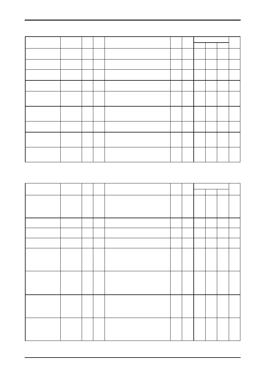
Electrical Characteristics at Ta = 25
°C
Recording mode Head Amplifier (T87:5.0V T11:5.0V)
Ratings
Parameter
Symbol
In
Out
Conditions
T13
T15
min
typ
max
Unit
Rec AGC Amp output
level
VRSP
VREP
T66A
T83A
T89A
Output level when VIN = 300mVp-p, f = 4MHz
Enter by applying DC 3.5V or more to pin 66.
0
5.0
127
104
135
111
143
119
mVp-p
Difference of gain
between mode
GVR
VRSP/VREP
1.40
1.7
2.00
dB
REC AGC AMP
control characteristics 1
VAGC1-SP
VAGC1-EP
T66A
T83A
T89A
Output level/VRSP, EP with
f = 4MHz and VIN = 700mVp-p
0
5.0
0.5
1.0
dB
REC AGC AMP
control characteristics 2
VAGC2-SP
VAGC2-EP
T66A
T83A
T89A
Output level/VRSP, EP with
f = 4MHz and VIN = 100mVp-p.
0
5.0
-1.0
-0.5
dB
REC AGC AMP
frequency
characteristics
VFRS
VFRE
T66A
T83A
T89A
The output ratio when f is 1M, 7MHz
as VIN = 300mVp-p.
7MHz/1MHz (Note 1)
0
5.0
-1.0
0.0
+1.0
dB
REC AGC AMP
second harmonic
distortion
VHDRS
VHDRE
T13A
T83A
T89A
The ratio of the 8Mz (second component) and
4Mz (first component) of the output with
VIN = 300mVp-p and f = 4MHz
0
5.0
-45
-40
dB
REC AGC AMP
maximum output level
VHDRS
VHDRE
T66A
T83A
T89A
The output level at which the second
distortion with f = 4MHz is -35dB.
0
5.0
20
22
mVp-p
REC AGC AMP
attenuate volume of
mute
VMRS
VMRE
T66A
T83A
T89A
Output level/VRSP, EP with
VIN = 300mVp-p and f = 4MHz
0
5.0
-45
-40
dB
REC AGC AMP
mixed modulation
relative level
VCYS
VCYE
T66A
T83A
T89A
Vin1 = 300mVp-p, f = 4MHz,
Vin2 = 300Vp-p, f = 629kHz (4M±629k)/4M
ratio of output
0
5.0
-45
-40
dB
Note1: Apply DC of about 1.6V to AGC detection filter terminal (Pin92), and fix the AGC amplifier gain.
Use a resistor with a tolerance of ±1.0% between Pin 93and GND.
PB mode Head Amplifier (T87 = 5.0V T11 = 0V)
Ratings
Parameter
Symbol
In
Out
Conditions
T13
T15
min
typ
max
Unit
SP-H
CH1
Gvp1
T82A
T74
0
56.0
59.0
62.0
dB
SP-H
CH2
Gvp2
T85A
5.0
0
56.0
59.0
62.0
EP-L
CH3
Gvp3
T88A
0
5.0
56.0
59.0
62.0
Voltage
gain
EP-H
CH4
Gvp4
T91A
VIN = 38mVp-p, f = 1MHz
5.0
56.0
59.0
62.0
Difference of
voltage gain 1
Gvp1
Gvp1 - Gvp2
-1
0
+1
dB
Difference of
voltage gain 2
Gvp2
Gvp3 - Gvp4
-1
0
+1
dB
Difference of gain
between mode
Gvp3
Gvp3 - Gvp1
-1
0
+1
dB
Input calculation
CH1
VNIN1
T82A
T74
0
0.7
1.0
Vrms
noise voltage
CH2
VNIN2
T85A
5.0
0
CH3
VNIN3
T88A
0
5.0
CH4
VNIN4
T91A
The ratio of the output which has passed the
1.1MHz LPF and the output without input
under the same input conditions as the
voltage gain.
5.0
Frequency
CH1
Vfp1
T82A
T74
0
-2.5
0
dB
characteristics
CH2
Vfp2
T85A
5.0
0
CH3
Vfp3
T88A
0
5.0
CH4
Vfp4
T91A
The ratio of the VIN = 38mVp-p,
f = 7MHz output and Gvp1, 2, 3, 4.
5.0
Secondary
CH1
VHDP1
T82A
T74
0
-40
-35
dB
harmonic
CH2
VHDP2
T85A
5.0
0
distortion
CH3
VHDP3
T88A
0
5.0
CH4
VHDP4
T91A
The ratio of 8MHz (second component) and
4MHz (first component) of output with
VIN = 38mVp-p and f = 4 MHz.
5.0
Maximum
CH1
VOMP1
T82A
T74
0
1.0
1.2
Vp-p
output level
CH2
VOMP2
T85A
5.0
0
CH3
VOMP3
T88A
0
5.0
CH4
VOMP4
T91A
The output level at which the ratio of 3MHz
(third component) and 1MHz (first
component) of the output with f = 1MHz.
5.0
Continued on next page.
相關(guān)PDF資料 |
PDF描述 |
|---|---|
| LA71076SM | SPECIALTY CONSUMER CIRCUIT, PQFP100 |
| LA7108M | 3 CHANNEL, VIDEO AMPLIFIER, PDSO16 |
| LA7109 | 6 CHANNEL, VIDEO AMPLIFIER, PDSO36 |
| LA7116 | SPECIALTY CONSUMER CIRCUIT, PDIP24 |
| LA71205M | SPECIALTY CONSUMER CIRCUIT, PQFP80 |
相關(guān)代理商/技術(shù)參數(shù) |
參數(shù)描述 |
|---|---|
| LA7108M-TLM-E | 制造商:Sony Semiconductor Solutions Division 功能描述: |
| LA7110 | 制造商:SANYO 制造商全稱:Sanyo Semicon Device 功能描述:VTR TAPE END DETECTOR |
| LA7110M | 制造商:未知廠家 制造商全稱:未知廠家 功能描述:Analog IC |
| LA7112M | 制造商:未知廠家 制造商全稱:未知廠家 功能描述:Analog IC |
| LA7116 | 制造商:SANYO 制造商全稱:Sanyo Semicon Device 功能描述:VCR Servo Interface |
發(fā)布緊急采購,3分鐘左右您將得到回復(fù)。