- 您現(xiàn)在的位置:買賣IC網(wǎng) > PDF目錄30720 > LA7138M SPECIALTY CONSUMER CIRCUIT, PDSO24 PDF資料下載
參數(shù)資料
| 型號(hào): | LA7138M |
| 元件分類: | 消費(fèi)家電 |
| 英文描述: | SPECIALTY CONSUMER CIRCUIT, PDSO24 |
| 封裝: | 0.300 INCH, MFP-24 |
| 文件頁數(shù): | 7/13頁 |
| 文件大?。?/td> | 320K |
| 代理商: | LA7138M |

LA7138M
No.A0220-3/16
Continued from preceding page.
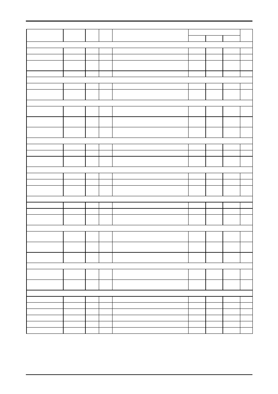
Ratings
Parameter
Symbol
Input
signal
Test
point
Conditions
min
typ
max
Unit
(H) Pin 6 (B-Y or R-Y signal) when the component is selected.
AMP-GAIN (Low)
GNM
Sig.4
T17/19
GAIN when 996mVp-p, 100 kHz is entered.
5.05
5.27
5.48
dB
AMP-GAIN (High)
GNH
Sig.4
T17/19
GAIN when 761mVp-p, 100 kHz is entered.
7.38
7.6
7.81
dB
Input pedestal clamp
voltage
P6H
Sig.4
T6
Potential of pedestal of T6 when 761mVp-p is
entered.
4.4
4.75
5.1
V
AMP-GAIN (Low)
GNM
Sig.4
T21/23
GAIN when 996mVp-p, 100 kHz is entered.
5.05
5.27
5.48
dB
(I) Pin 3 (B-Y or R- Y signal) input when the component is selected.
AMP-GAIN (High)
GNH
Sig.4
T21/23
GAIN when 761mVp-p, 100 kHz is selected.
7.38
7.6
7.81
dB
Input pedestal clamp
voltage
P3H
Sig.4
T3
Potential of pedestal of T3 when 761mVp-p is
entered.
4.4
4.75
5.1
V
(J) GAIN ratio of signals when the component is selected.
Y/composite-AMP-
GAIN ratio (1)
Y1
Sig.1
Sig.4
T13/15
T17/19
GAIN ratio between GYH of (E) and GNH of (F)
-3
0
3
%
Y/composite-AMP-
GAIN ratio (2)
Y2
Sig.1
Sig.4
T13/15
T21/23
GAIN ratio between GYH of (E) and GNH of (G)
-3
0
3
%
Component-AMP-
GAIN ratio
N
Sig.4
T17/19
T21/23
GAIN ratio between GNH of (F) and that of (G)
-3
0
3
%
(K) Pin 10 (RGB signal) input when the base band is selected.
AMP-GAIN (Low)
GBM
Sig.1
T13/15
GAIN when 996mVp-p, 100 kHz is entered.
5.05
5.27
5.48
dB
AMP-GAIN (High)
GBH
Sig.1
T13/15
GAIN when 761mVp-p, 100 kHz is entered.
7.38
7.6
7.81
dB
Input clamp voltage
C10H
Sig.1
T10
Potential of sink chip of T10 when 761mVp-p is
entered.
3.85
4.20
4.55
V
(L) Pin 6 (RGB signal) Input when the base band is entered.
AMP-GAIN (Low)
GBM
Sig.1
T13/15
GAIN when 996mVp-p, 100 kHz is entered.
5.05
5.27
5.48
dB
AMP-GAIN (High)
GBH
Sig.1
T13/15
GAIN when 761mVp-p, 100 kHz is entered.
7.38
7.6
7.81
dB
Input clamp voltage
C6H
Sig.1
T10
Potential of sink chip of T10 when 761mVp-p is
entered.
4.0
4.35
4.7
V
(M) Pin 3 (RGB signal) Input when the base band is entered.
AMP-GAIN (Low)
GBM
Sig.1
T13/15
GAIN when 996mVp-p, 100 kHz is entered.
5.05
5.27
5.48
dB
AMP-GAIN (High)
GBH
Sig.1
T13/15
GAIN when 761mVp-p, 100 kHz is entered.
7.38
7.6
7.81
dB
Input clamp voltage
C3H
Sig.1
T10
Potential of sink chip of T10 when 761mVp-p is
entered.
4.0
4.35
4.7
V
(N) GAIN ratio of signals when the base band is selected.
Base bank –AMP-
GAIN ratio (1)
B1
Sig.1
T13/15
T17/19
GAIN ratio between GBH of (I) and that of (J)
-3
0
3
%
Base band –AMP-
GAIN ratio (2)
B2
Sig.1
T13/15
T21/23
GAIN ratio between GBH of (I) and that of (K)
-3
0
3
%
Base band –AMP-
GAIN ratio
B3
Sig.1
T17/19
T21/23
GAIN ratio between GBH of (J) and that of (K)
-3
0
3
%
(O) f characteristics of GAIN (common to all modes and input signals, however, except for Y/C-MIX).
LPF 6MHz
attenuation
FY6
Sig.1
T13/15
Difference between GAIN and GYH
when 761mVp-p, 6MHz is entered.
-0.5
0
+0.5
dB
LPF 10MHz
attenuation
FY10
Sig.1
T13/15
Difference between GAIN and GYH
when 761mVp-p, 10MHz is entered.
-0.5
0
+0.5
dB
(P) DC voltage for output mute (common to all modes).
Pin 13 voltage
V13
T13
3.7
4.05
4.4
V
Pin 15 voltage
V15
T15
3.7
4.05
4.4
V
Pin 17 voltage
V17
T17
3.9
4.25
4.6
V
Pin 19 voltage
V19
T19
3.9
4.25
4.6
V
Pin 21 voltage
V21
T21
3.9
4.25
4.6
V
Pin 23 voltage
V23
T23
3.9
4.25
4.6
V
Continued on next page.
相關(guān)PDF資料 |
PDF描述 |
|---|---|
| LA71521M | SPECIALTY CONSUMER CIRCUIT, PQFP80 |
| LA71578HM | SPECIALTY CONSUMER CIRCUIT, PQFP100 |
| LA71582M | SPECIALTY CONSUMER CIRCUIT, PQFP100 |
| LA71582M | SPECIALTY CONSUMER CIRCUIT, PQFP100 |
| LA71584M | FM, AUDIO/VIDEO DEMODULATOR, PQFP100 |
相關(guān)代理商/技術(shù)參數(shù) |
參數(shù)描述 |
|---|---|
| LA7140 | 制造商:未知廠家 制造商全稱:未知廠家 功能描述: |
| LA7150 | 制造商:SANYO 制造商全稱:Sanyo Semicon Device 功能描述:Audio/Video Switch for PAL System VCR |
| LA7151 | 制造商:SANYO 制造商全稱:Sanyo Semicon Device 功能描述:Audio/Video Switch for VCR Video Camera Use |
| LA7151M | 制造商:SANYO 制造商全稱:Sanyo Semicon Device 功能描述:Audio/Video Switch for VCR Video Camera Use |
| LA7152 | 制造商:SANYO 制造商全稱:Sanyo Semicon Device 功能描述:VCR Electronic Switch |
發(fā)布緊急采購(gòu),3分鐘左右您將得到回復(fù)。