- 您現(xiàn)在的位置:買(mǎi)賣(mài)IC網(wǎng) > PDF目錄30722 > LA72914V (SANYO SEMICONDUCTOR CO LTD) SPECIALTY CONSUMER CIRCUIT, PDSO16 PDF資料下載
參數(shù)資料
| 型號(hào): | LA72914V |
| 廠商: | SANYO SEMICONDUCTOR CO LTD |
| 元件分類(lèi): | 消費(fèi)家電 |
| 英文描述: | SPECIALTY CONSUMER CIRCUIT, PDSO16 |
| 封裝: | 0.225 INCH, SSOP-16 |
| 文件頁(yè)數(shù): | 2/9頁(yè) |
| 文件大?。?/td> | 290K |
| 代理商: | LA72914V |
LA72914V
No.A1859-2/9
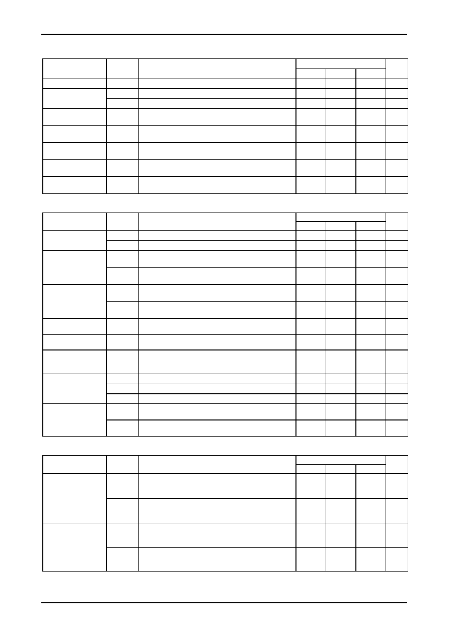
Electrical Characteristics at Ta
= 25°C, VCC = 5V
DC Characteristic
Ratings
Parameter
Symbol
Conditions
min
typ
max
Unit
2.4V regulator
VREG
Measure the DC voltage at pin 2
2.2
2.4
2.6
V
ICC1
Measure the current into pin 4 in normal mode.
26.0
33.0
40.0
mA
Current dissipation
ICC2
Measure the current into pin 4 in stand-by mode.
2.0
2.5
3.0
mA
Control pin (6 pin)
Low level
CNT6L
Low level of input pin (6pin) in 4.5MHz TX mode.
0
0.4
V
Control pin (6 pin)
Middle level
CNT6M
Middle level of input pin (6pin) in stand-by mode.
2.0
3.0
V
Control pin (6 pin)
High level
CNT6H
High level of input pin (6pin) in 6.5MHz TX mode.
4.5
5.0
V
AGC stop at pin 11
control voltage
AGCS
Voltage of input pin (pin 11) in AGC stop
4.5
5.0
V
TX OFF mode at pin 16
control voltage
CNT16L
Voltage of input pin (pin 16) in TX off mode
0
0.4
V
Sound FM Modulation Block (TX)
Ratings
Parameter
Symbol
Conditions
min
typ
max
Unit
FFM1
Output frequency of T1B in no signals. T6=0.6V, T14:open
4.455
4.500
4.545
MHz
FM carrier
output frequency
FFM2
Output frequency of T1B in no signals. T6=4.2V, T14:open
6.435
6.500
6.565
MHz
VOFM1
Output level of T1B in no signals.
Load impedance = 1k
Ω T1-GND. T6=0.6V
1.9
2.3
2.6
Vp-p
FM carrier output level
VOFM2
Output level of T1B in no signals.
Load impedance = 1k
Ω T1-GND. T6=4.2V
1.3
1.7
2.1
Vp-p
2HD1
2
nd harmonics distortion of T1B in no signals.
Load impedance = 1k
Ω T1-GND. T6=0.6V
-30
-20
dB
FM carrier output
second harmonics
distortion
2HD2
2
nd harmonics distortion of T1B in no signals.
Load impedance = 1k
Ω T1-GND. T6=4.2V
-30
-20
dB
FM carrier output mute
level
VFMT
Output level of T1B in TX off mode. T6=0.6V (4.2V)
-60
-50
dB
FM deviation
DEV
FM deviation of T1A, T6=0.6V (4.2V), input at
T16=1.0Vp-p/1kHz (sine)
20
25
30
kHz
Emphasis
Characteristic
FEMP
T16=200mVp-p, 1kHz (sine), M1=T1 output deviation.
T16=200mVp-p, 5kHz (sine), M2=T1 output deviation.
FEMP=M2-M1
7
12
17
kHz
ALC1
T16A=0.25Vp-p, 1kHz (sine), T3:Open, T6=0.6V, T3 output level
0.45
0.5
0.55
Vp-p
ALC2
T16A=0.6Vp-p, 1kHz (sine), T3:Open, T6=0.6V, T3 output level
0.9
1.0
1.1
Vp-p
ALC characteristic
ALC3
T16A=1.0Vp-p, 1kHz (sine), T3:Open, T6=0.6V, T3 output level
0.95
1.05
1.15
Vp-p
FCNT1
No signal input. Measure T1B frequency. T16:Open, T6=0.6V
(4.2V), T14=0.5V
-0.22
MHz
FM carrier “fo”
adjustment (reference)
FCNT2
No signal input. Measure T1B frequency. T16:Open, T6=0.6V
(4.2V), T14=4.5V
+-.22
MHz
Sound FM demodulation block (RX)
Ratings
Parameter
Symbol
Conditions
min
typ
max
Unit
VOUT1
Input signal: CAR=4.5MHz, DEV=
±25kHz, MOD=1kHz,
Level: 100mVp-p. T5A input. Measure T9B signal level.
(T9B-GND: ROUT=10kΩ) T6=4.2V
0.6
0.9
1.3
Vp-p
Sound demodulation
level
VOUT2
Input signal: CAR=6.5MHz, DEV=
±25kHz, MOD=1kHz,
Level: 100mVp-p. T5A input. Measure T9B signal level.
(T9B-GND: ROUT =10kΩ) T6=0.6V
0.7
1.0
1.4
Vp-p
SN1
Input signal: CAR=4.5MHz, No-modulation. Level: 100mVp-p.
T5A input. T6=4.2V, (IHF-A) M1=T9B signal level. (T9B-GND:
ROUT =10kΩ) SN1=20log(VOUT1/M1)
35
50
dB
S/N
SN2
Input signal: CAR=6.5MHz, No-modulation. Level: 100mVp-p.
T5A input. T6=0.6V, (IHF-A) M1=T9B signal level. (T9B-GND:
ROUT =10kΩ) SN1=20log(VOUT2/M1)
35
50
dB
Continued on next page
相關(guān)PDF資料 |
PDF描述 |
|---|---|
| LA7300M | 3 CHANNEL, VIDEO PREAMPLIFIER, PDSO24 |
| LA7301M | 4 CHANNEL, VIDEO PREAMPLIFIER, PDSO30 |
| LA7301 | 4 CHANNEL, VIDEO PREAMPLIFIER, PDIP30 |
| LA73026AV | SPECIALTY CONSUMER CIRCUIT, PDSO44 |
| LA73026AV | SPECIALTY CONSUMER CIRCUIT, PDSO44 |
相關(guān)代理商/技術(shù)參數(shù) |
參數(shù)描述 |
|---|---|
| LA72914VL-TLM-H | 功能描述:調(diào)節(jié)器/解調(diào)器 RoHS:否 制造商:Texas Instruments 封裝 / 箱體:PVQFN-N24 封裝:Reel |
| LA72914V-MPB-H | 功能描述:調(diào)節(jié)器/解調(diào)器 RoHS:否 制造商:Texas Instruments 封裝 / 箱體:PVQFN-N24 封裝:Reel |
| LA72914V-TLM-H | 功能描述:調(diào)節(jié)器/解調(diào)器 RoHS:否 制造商:Texas Instruments 封裝 / 箱體:PVQFN-N24 封裝:Reel |
| LA7293 | 制造商:未知廠家 制造商全稱(chēng):未知廠家 功能描述: |
| LA7293M | 制造商:SANYO 制造商全稱(chēng):Sanyo Semicon Device 功能描述:Microphone Amplifier for Video Cameras |
發(fā)布緊急采購(gòu),3分鐘左右您將得到回復(fù)。