- 您現(xiàn)在的位置:買賣IC網(wǎng) > PDF目錄358740 > LA9230M (Sanyo Electric Co.,Ltd.) Analog Signal Processor ASP for CD players PDF資料下載
參數(shù)資料
| 型號: | LA9230M |
| 廠商: | Sanyo Electric Co.,Ltd. |
| 英文描述: | Analog Signal Processor ASP for CD players |
| 中文描述: | 模擬信號處理器的平均銷售CD播放機(jī) |
| 文件頁數(shù): | 3/20頁 |
| 文件大小: | 227K |
| 代理商: | LA9230M |
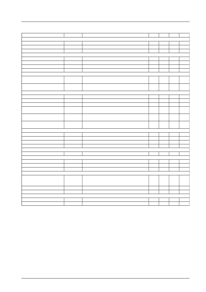
Continued from preceding page.
Parameter
Symbol
Conditions
min
typ
max
Unit
[HFL]
Detection voltage
Output voltage H
Output voltage L
[TES]
Detection voltage LH
Detection voltage HL
Output voltage H
Output voltage L
[JP]
HFLvth
HFL-H
HFL-L
Difference from VR at RFSM
–0.35
4.5
–0.2
4.9
–0.05
V
0
+0.5
V
TES-LH
TES-HL
TES-H
TES-L
TESI, difference from VR
TESI, difference from VR
–0.15
0.05
4.5
–0.10
0.10
4.9
–0.05
0.15
V
V
V
V
0
+0.5
Output voltage H
JP-H
Difference from JP
+
= 0 V, JP
–
= 0 V at JP
+
= 0 V,
JP
–
= 5 V, TO
Difference from JP
+
= 0 V, JP
–
= 0 V at JP
+
= 5 V,
JP
–
= 0 V, TO
0.35
0.5
0.65
V
Output voltage L
JP-L
–0.65
–0.5
–0.35
V
[Spindle amplifier]
Offset 12
Offset 8
Offset off
SPD12ost
SPD8ost
SPDof
Difference from VR at SPD, 12 cm mode
Difference from VR at SPD, 8 cm mode
Difference from VR at SPD, OFF mode
Difference from offset-12, 12 cm mode
CV
+
= 5 V, CV
–
= 0 V
Difference from offset-12 , 12 cm mode
CV
+
= 0 V, CV
–
= 5 V
Difference from offset-8, 8 cm mode
CV
+
= 5 V, CV
–
= 0 V
–40
–40
–30
0
0
0
+40
+40
+30
mV
mV
mV
Output voltage H12
SPD-H12
0.75
1.0
1.25
V
Output voltage L12
SPD-L12
–1.25
–1.0
–0.75
V
Output voltage H8
SPD-H8
0.35
0.5
0.65
V
[Sled amplifier]
SLEQ offset
Offset SLD
Offset off
Off VTH
[SLC]
No signal voltage
[Shock]
No signal voltage
Detection voltage H
Detection voltage L
[DEF]
SLEQost
SLDost
SLDof
SLOFvth
Difference from TO at SLEQ
SLEQ = VR, difference from VR
Off mode
SLOF
–30
–100
–40
1.0
0
0
0
+30
+100
+40
2.0
mV
mV
mV
V
1.4
SLCo
SLC
2.25
2.5
2.75
V
SCIo
SCIvthH
SCIvthL
SCI, difference from VR
SCI, difference from VR
SCI, difference from VR
–40
60
–140
0
+40
140
–60
mV
mV
mV
100
–100
Detection voltage
DEFvth
Difference between LF2 voltage when RFSM =
3.5 V and DEF is detected and LF2 voltage when
RFSM = 3.5 V
0.20
0.35
0.50
V
Output voltage H
Output voltage L
[APC]
Reference voltage
Off voltage
DEF-H
DEF-L
4.5
4.9
V
V
0
+0.5
LDS
LDDof
LDS voltage at which LDD = 3 V
LDD
150
3.9
180
4.3
210
4.6
mV
V
LA9230M/9231M
No.5189 - 3/20
相關(guān)PDF資料 |
PDF描述 |
|---|---|
| LA9233 | Analog Signal Processor ASP for CD players |
| LA9233M | Analog Signal Processor ASP for CD players |
| LA9240M | Analog Signal Processor (ASP) for CD players |
| LA9241M | Analog Signal Processor ASP for CD players |
| LA9242M | Analog Signal Processor ASP for CD Players |
相關(guān)代理商/技術(shù)參數(shù) |
參數(shù)描述 |
|---|---|
| LA9231 | 制造商:SANYO 制造商全稱:Sanyo Semicon Device 功能描述:Analog Signal Processor ASP for CD players |
| LA9231M | 制造商:SANYO 制造商全稱:Sanyo Semicon Device 功能描述:Analog Signal Processor ASP for CD players |
| LA9233 | 制造商:SANYO 制造商全稱:Sanyo Semicon Device 功能描述:Analog Signal Processor ASP for CD players |
| LA9233M | 制造商:SANYO 制造商全稱:Sanyo Semicon Device 功能描述:Analog Signal Processor ASP for CD players |
| LA9235M | 制造商:未知廠家 制造商全稱:未知廠家 功能描述: |
發(fā)布緊急采購,3分鐘左右您將得到回復(fù)。