- 您現(xiàn)在的位置:買賣IC網(wǎng) > PDF目錄43902 > LB1870 BRUSHLESS DC MOTOR CONTROLLER, 1 A, PDIP28 PDF資料下載
參數(shù)資料
| 型號: | LB1870 |
| 元件分類: | 運動控制電子 |
| 英文描述: | BRUSHLESS DC MOTOR CONTROLLER, 1 A, PDIP28 |
| 封裝: | HSDIP-28 |
| 文件頁數(shù): | 11/11頁 |
| 文件大小: | 108K |
| 代理商: | LB1870 |

8. Oscillator pin
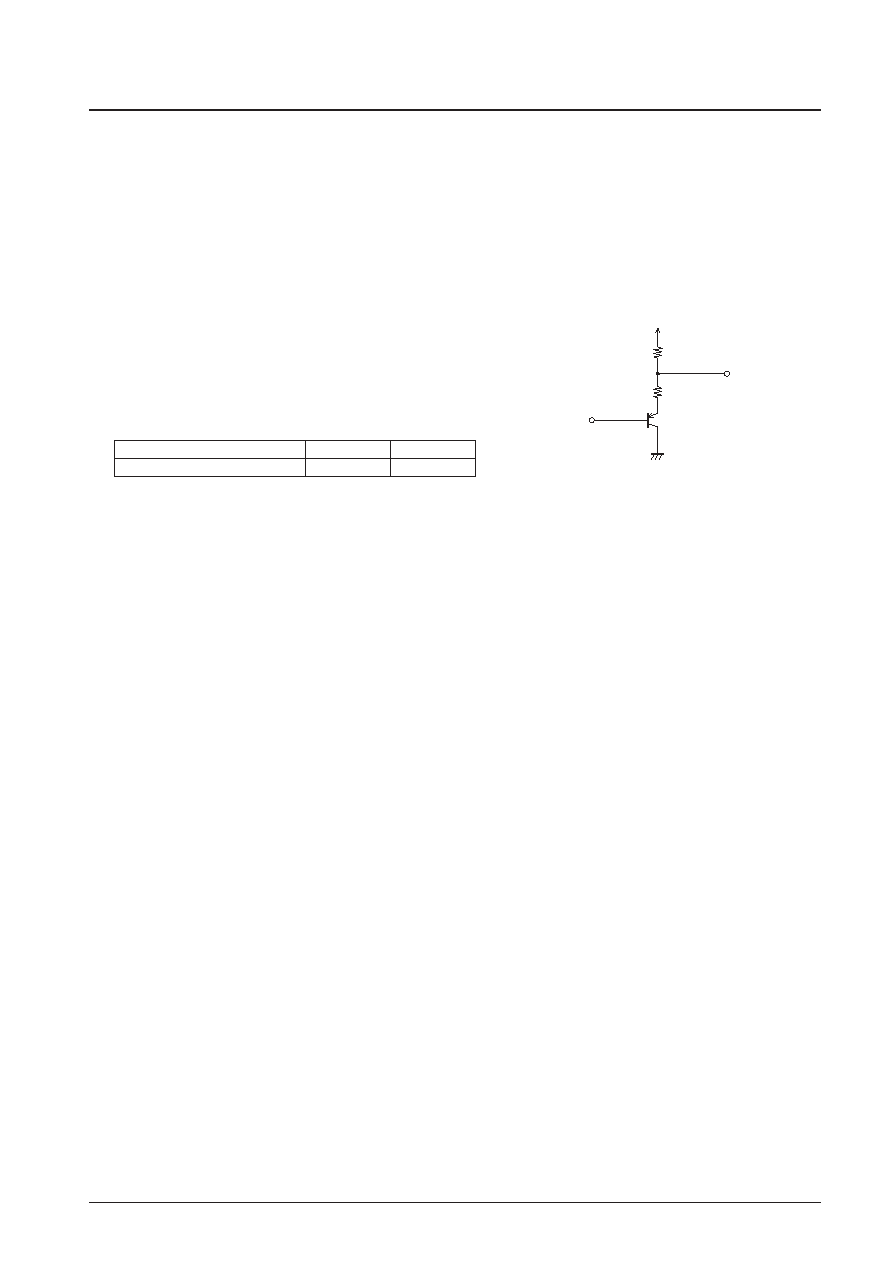
A crystal oscillator and an RC circuit is connected to the LB1870’s
OSC pin. To avoid problems when selecting the oscillator and the
capacitor and resistor values, confirm these values with the
oscillator’s manufacturer. The pnp transistor and resistor circuit
shown in the figure can be used to apply an external signal (of a
few MHz) to the OSC pin.
fin = 1 to 8 MHz
Input signal level: High level voltage: 4.0 V minimum
Low level voltage: 1.5 V maximum
It will be necessary to insert a capacitor of a certain size if there is
overshoot or undershoot in the input waveform. Contact your
Sanyo representative for more information on this point if
necessary.
Use the LB1870 VREG output for the VDD = 6.3 V case.
9. IC internal power dissipation calculation example (calculated at VCC = 24 V, standard ratings)
Power dissipation due to current drain
P1 = VCC × ICC = 24 V × 22 mA = 0.53 W
Power dissipation when a –10 mA load current is drawn from the 6.3 V fixed voltage power supply.
P2 = (VCC – VREG) × I load = 17.7 V × 10 mA = 0.18 W
Power dissipation due to the output drive current
(When IO = 0.1 A, the inter-coil voltage V Rm = Rm × IO, and the reverse voltage = 15 V)
P3 = (IO/100) × [(VCC – 0.7 V) + ((VCC – V Rm)/2) – 0.7 V] + VCC2/16 k
= 1 mA
× (23.3 V + 3.8 V) + 24 V2/16 k = 0.06 W
Power dissipation due to the output transistor
(When IO = 0.1 A, the inter-coil voltage V Rm = Rm × IO, and the reverse voltage = 15 V)
P4 = (VCC – V Rm) × IO = 9 V × 0.1 A = 0.9 W
Therefore, the IC’s total power dissipation is:
In stop mode:
P = P1 + P2 = 0.71 W
In start mode (When IO = 0.1 A, the inter-coil voltage V Rm = Rm × IO, and the reverse voltage = 15 V)
P = P1 + P2 + P3 + P4 = 1.67 W
No. 4356-9/11
LB1870, 1870M
VDD = 6.3 V typ. (5.8 to 6.8 V)
Ra = 4.7 k
Rb = 1.3 k
VDD = 5.0 V typ. (4.5 to 5.5 V)
Ra = 2.0 k
Rb = 1.0 k
VDD
Rb
Ra
for OSC pin
Input
相關(guān)PDF資料 |
PDF描述 |
|---|---|
| LB1870 | BRUSHLESS DC MOTOR CONTROLLER, 1 A, PDIP28 |
| LB1871 | BRUSHLESS DC MOTOR CONTROLLER, 1 A, PDIP28 |
| LB1876 | BRUSHLESS DC MOTOR CONTROLLER, 2.5 A, PDSO36 |
| LB1876 | BRUSHLESS DC MOTOR CONTROLLER, 2.5 A, PDSO36 |
| LB1921 | BRUSHLESS DC MOTOR CONTROLLER, 3.5 A, PDIP28 |
相關(guān)代理商/技術(shù)參數(shù) |
參數(shù)描述 |
|---|---|
| LB1870M | 制造商:SANYO 制造商全稱:Sanyo Semicon Device 功能描述:Three-Phase Brushless Motor Driver |
| LB1871 | 制造商:SANYO 制造商全稱:Sanyo Semicon Device 功能描述:Three-Phase Brushless Motor Driver |
| LB1871M | 制造商:SANYO 制造商全稱:Sanyo Semicon Device 功能描述:Three-Phase Brushless Motor Driver |
| LB1872 | 制造商:SANYO 制造商全稱:Sanyo Semicon Device 功能描述:Polygon Mirror Scanner Driver IC |
| LB1875 | 制造商:SANYO 制造商全稱:Sanyo Semicon Device 功能描述:Polygon Mirror Motor Predriver IC |
發(fā)布緊急采購,3分鐘左右您將得到回復。