Lattice Semiconductor
ispMACH 4000V/B/C/Z Family Data Sheet
25
Timing Model
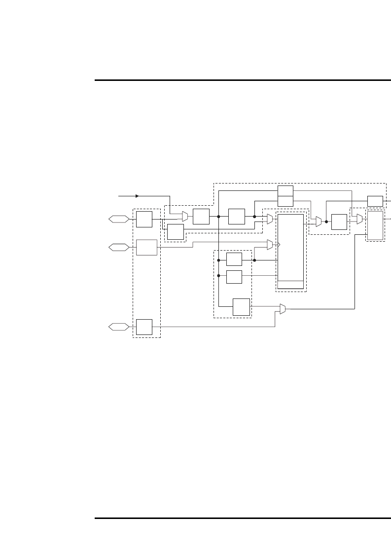
The task of determining the timing through the ispMACH 4000 family, like any CPLD, is relatively simple. The timing
model provided in Figure 11 shows the speci
fi
c delay paths. Once the implementation of a given function is deter-
mined either conceptually or from the software report
fi
le, the delay path of the function can easily be determined
from the timing model. The Lattice design tools report the timing delays based on the same timing model for a par-
ticular design. Note that the internal timing parameters are given for reference only, and are not tested. The exter-
nal timing parameters are tested and guaranteed for every device. For more information on the timing model and
usage, please refer to Technical Note TN1004:
ispMACH 4000 Timing Model Design and Usage Guidelines.
Figure 11. ispMACH 4000 Timing Model
DATA
MC Reg.
C.E.
S/R
Q
SCLK
IN
OE
In/Out
Delays
In/Out
Delays
Control
Delays
Register/Latch
Delays
Routing/GLB Delays
Note: Italicized items are optional delay adders.
t
FBK
Feedback
From
Feedback
t
BUF
t
IOO
t
EN
t
DIS
t
PDb
t
MCELL
t
EXP
t
PTCLK
t
BCLK
t
PTSR
t
BSR
t
GPTOE
t
PTOE
t
ROUTE
t
BLA
t
INREG
t
INDIO
t
IN
t
IOI
t
GCLK_IN
t
IOI
t
GOE
t
IOI
t
PDi
t
ORP