- 您現(xiàn)在的位置:買賣IC網(wǎng) > PDF目錄30730 > LC723341E (SANYO SEMICONDUCTOR CO LTD) SPECIALTY CONSUMER CIRCUIT, PQFP64 PDF資料下載
參數(shù)資料
| 型號(hào): | LC723341E |
| 廠商: | SANYO SEMICONDUCTOR CO LTD |
| 元件分類: | 消費(fèi)家電 |
| 英文描述: | SPECIALTY CONSUMER CIRCUIT, PQFP64 |
| 封裝: | 14 X 14 MM, 0.80 MM PITCH, QIP-64 |
| 文件頁(yè)數(shù): | 2/11頁(yè) |
| 文件大小: | 114K |
| 代理商: | LC723341E |

LC723341E
No.8013-10/11
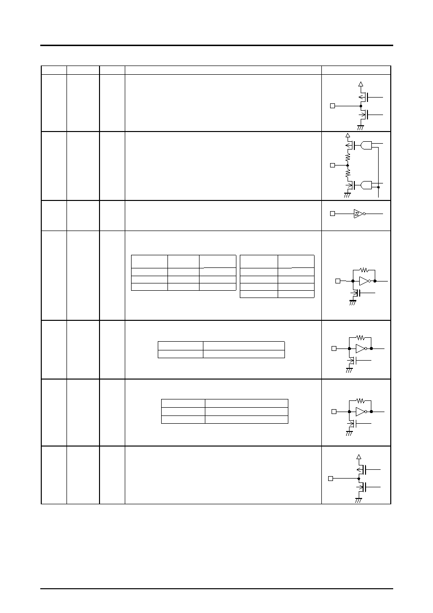
Continued from preceding page.
Pin No.
Symbol
I/O
Description
Equivalent circuit
48-37
S1-S12
O
LCD driver segment output pins.
This driver implements 1/4-duty 1/2-bias drive.
The frame frequency is 75 Hz.
In backup mode, after a reset, and after an LCD off instruction has been executed, these
pins will be held fixed at the low level.
CMOS push-pull circuit
62
61
60
59
COM1
COM2
COM3
COM4
O
LCD driver common output pins.
This driver implements 1/4-duty 1/2-bias drive.
The frame frequency is 75 Hz.
In backup mode, after a reset, and after an LCD off instruction has been executed, these
pins will be held fixed at the low level.
69
BRES
System reset pin.
If this pin is held low for at least one machine cycle during CPU operation or in halt mode,
the system will be reset and execution will continue with the program counter set to location
0.
54
HCTR
I
Dedicated universal counter input port.
For frequency measurement, select frequency measurement mode with the UCD
instruction (b3 = 0, b2 = 0) and start the counter with the UCC instruction.
The CNTEND flag will be set when the count completes. In this mode, the input operates as
an AC amplifier. Thus the input must be capacitance coupled. Input is disabled in backup
mode, in halt mode, during a reset, and in PLL stop mode.
CMOS amplifier input
56
FMIN
I
FM VCO (local oscillator) input.
This pin is selected using the PLL instruction CW1 field.
The input must be capacitor coupled.
Input is disabled in backup mode, in halt mode, during a reset, and in PLL stop mode.
CMOS amplifier input
57
AMIN
I
AM VCO (local oscillator) input.
This pin is selected and the bandwidth set using the PLL instruction CW1 field.
The input must be capacitor coupled.
Input is disabled in backup mode, in halt mode, during a reset, and in PLL stop mode.
CMOS amplifier input
59
EO
O
This is the main charge pump output. When the frequency of the local oscillator divided by N
is higher than the reference frequency, a high level is output, and when it is lower, a low level
is output. This pin goes to the high-impedance state when the frequencies match.
This pin goes to the output high-impedance state in backup mode, in halt mode, during a
reset, and in PLL stop mode.
CMOS push-pull circuit
Continued on next page.
Measurement
time
1
0
1
32 ms
8 ms
4 ms
1 ms
0
UCS b1, b0
Measurement
time
1
0
1
HCTR
0
Measurement
mode
Frequency
UCS b3, b2
0
Band
10 to 250 MHz
CW1 b1, b0
1
0
Band
0.5 to 10 MHz (MW,LW)
CW1 b1, b0
1
2 to 40 MHz (SW)
相關(guān)PDF資料 |
PDF描述 |
|---|---|
| LC723341E | SPECIALTY CONSUMER CIRCUIT, PQFP64 |
| LC7234-8460 | SPECIALTY CONSUMER CIRCUIT, PQFP64 |
| LC723401W-XXXX | SPECIALTY CONSUMER CIRCUIT, PQFP64 |
| LC723401W-XXXX | SPECIALTY CONSUMER CIRCUIT, PQFP64 |
| LC72342-XXXX | SPECIALTY CONSUMER CIRCUIT, PQFP64 |
相關(guān)代理商/技術(shù)參數(shù) |
參數(shù)描述 |
|---|---|
| LC72336 | 制造商:SANYO 制造商全稱:Sanyo Semicon Device 功能描述:Single-Chip Microcontrollers with Built-In LCD Driver and PLL Circuits |
| LC72338 | 制造商:SANYO 制造商全稱:Sanyo Semicon Device 功能描述:Single-Chip Microcontrollers with Built-In LCD Driver and PLL Circuits |
| LC7233N | 制造商:SANYO 制造商全稱:Sanyo Semicon Device 功能描述:Single-Chip PLL and Microcontroller with LCD Driver |
| LC7233N-8818 | 制造商:SANYO 制造商全稱:Sanyo Semicon Device 功能描述:Single-Chip PLL and Controller with LCD Driver |
| LC7234 | 制造商:SANYO 制造商全稱:Sanyo Semicon Device 功能描述:Single-Chip PLL and Microcontroller with LCD Driver |
發(fā)布緊急采購(gòu),3分鐘左右您將得到回復(fù)。