- 您現(xiàn)在的位置:買賣IC網(wǎng) > PDF目錄30731 > LC72710LW SPECIALTY CONSUMER CIRCUIT, PQFP64 PDF資料下載
參數(shù)資料
| 型號: | LC72710LW |
| 元件分類: | 消費(fèi)家電 |
| 英文描述: | SPECIALTY CONSUMER CIRCUIT, PQFP64 |
| 封裝: | 10 X 10 MM, SQFP-64 |
| 文件頁數(shù): | 7/7頁 |
| 文件大?。?/td> | 168K |
| 代理商: | LC72710LW |

LC72710W, 72710LW
No.6166-7/30
Continued from preceding page.
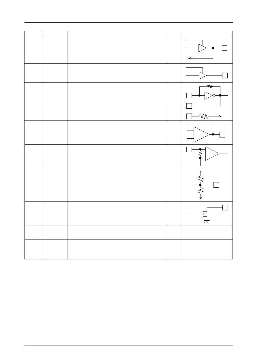
Pin No.
Pin
Function
I/O
Pin circuit
Data bus
17 to 24
D0 to D7
The bus width can be set to be either 8 bits or 16bits by the BUSWD
I/O
pin (pin 48).
For data input, only the lower 8 bits (D0 to D7) are valid.
25 to 32
D8 to D15
Data bus (in 16-bit mode)
Output
These pins are held in the output off state when BUSWD is low.
64
XIN
Connections for the system clock crystal oscillator circuit.
I/O
1
XOUT
The XIN pin can also be used as an external clock signal input.
53
MPXIN
Baseband (multiplex) signal input
Input
55
FLOUT
Subcarrier output (76kHz bandpass filter output)
Output
56
CIN
Subcarrier input (comparator input)
Input
52
VREF
Reference voltage output (Vdda/2)
Output
36
DO
CCB serial interface data output
Output
37
50
NC
This pin must be left open
57
54
VDDA
Analog system power supply
-
51
VSSA
Analog system ground
-
2, 15, 34
VDDD
Digital system power supply (+4.5V to +5.5V)
-
14, 35, 63
VSSD
Digital system ground
-
Notes: 1. This pin must be connected to VDDD or VSSD if the IC is used in serial interface mode (when SP is high).
2. A capacitor of at least 2000pF must be inserted between VDDD and VSSD.
Control Registers
This IC includes both registers that can be read and registers that can be written. These registers can be accessed using
either the serial interface (CCB) or the parallel interface. The SP pin switches between these interfaces.
The initial values of the write registers are the data loaded into internal registers when a reset signal (RST) is received.
These values are recommended values that do not need to be changed during normal operation.
If the parallel interface is used, applications must hold the address fixed at 00H when reading out data to which error
correction has been applied. If the CCB interface is used, the application needs only to specify the CCB address (#FB).
The address 00H is an invalid address for writing.
The addresses other than those specified below are control addresses particular to the IC. Applications must not specify
those addresses.
Continued on next page.
--
+
Vref
--
+
Vssa
Vdda
相關(guān)PDF資料 |
PDF描述 |
|---|---|
| LC72710W | SPECIALTY CONSUMER CIRCUIT, PQFP64 |
| LC72710LW | SPECIALTY CONSUMER CIRCUIT, PQFP64 |
| LC72710W | SPECIALTY CONSUMER CIRCUIT, PQFP64 |
| LC72711LW | SPECIALTY CONSUMER CIRCUIT, PQFP64 |
| LC72711W | SPECIALTY CONSUMER CIRCUIT, PQFP64 |
相關(guān)代理商/技術(shù)參數(shù) |
參數(shù)描述 |
|---|---|
| LC72710W | 制造商:SANYO 制造商全稱:Sanyo Semicon Device 功能描述:Mobile FM Multiplex Broadcast DARC Receiver IC with On-Chip VICS Decoder |
| LC72711LW | 制造商:SANYO 制造商全稱:Sanyo Semicon Device 功能描述:Mobile FM Multiplex Broadcast DARC Receiver IC |
| LC72711LW-E | 制造商:ON Semiconductor 功能描述:DARC DECODE-LSI - Trays |
| LC72711LWHS-E | 功能描述:射頻接收器 RoHS:否 制造商:Skyworks Solutions, Inc. 類型:GPS Receiver 封裝 / 箱體:QFN-24 工作頻率:4.092 MHz 工作電源電壓:3.3 V 封裝:Reel |
| LC72711W | 制造商:SANYO 制造商全稱:Sanyo Semicon Device 功能描述:Mobile FM Multiplex Broadcast DARC Receiver IC |
發(fā)布緊急采購,3分鐘左右您將得到回復(fù)。