- 您現(xiàn)在的位置:買賣IC網(wǎng) > PDF目錄21970 > LFEC20E-5F484C (Lattice Semiconductor Corporation)IC FPGA 19.7KLUTS 360I/O 484-BGA PDF資料下載
參數(shù)資料
| 型號: | LFEC20E-5F484C |
| 廠商: | Lattice Semiconductor Corporation |
| 文件頁數(shù): | 115/163頁 |
| 文件大小: | 0K |
| 描述: | IC FPGA 19.7KLUTS 360I/O 484-BGA |
| 標準包裝: | 60 |
| 系列: | EC |
| 邏輯元件/單元數(shù): | 19700 |
| RAM 位總計: | 434176 |
| 輸入/輸出數(shù): | 360 |
| 電源電壓: | 1.14 V ~ 1.26 V |
| 安裝類型: | 表面貼裝 |
| 工作溫度: | 0°C ~ 85°C |
| 封裝/外殼: | 484-BBGA |
| 供應商設備封裝: | 484-FPBGA(23x23) |
| 其它名稱: | 220-1287 LFEC20E-5F484C-ND |
第1頁第2頁第3頁第4頁第5頁第6頁第7頁第8頁第9頁第10頁第11頁第12頁第13頁第14頁第15頁第16頁第17頁第18頁第19頁第20頁第21頁第22頁第23頁第24頁第25頁第26頁第27頁第28頁第29頁第30頁第31頁第32頁第33頁第34頁第35頁第36頁第37頁第38頁第39頁第40頁第41頁第42頁第43頁第44頁第45頁第46頁第47頁第48頁第49頁第50頁第51頁第52頁第53頁第54頁第55頁第56頁第57頁第58頁第59頁第60頁第61頁第62頁第63頁第64頁第65頁第66頁第67頁第68頁第69頁第70頁第71頁第72頁第73頁第74頁第75頁第76頁第77頁第78頁第79頁第80頁第81頁第82頁第83頁第84頁第85頁第86頁第87頁第88頁第89頁第90頁第91頁第92頁第93頁第94頁第95頁第96頁第97頁第98頁第99頁第100頁第101頁第102頁第103頁第104頁第105頁第106頁第107頁第108頁第109頁第110頁第111頁第112頁第113頁第114頁當前第115頁第116頁第117頁第118頁第119頁第120頁第121頁第122頁第123頁第124頁第125頁第126頁第127頁第128頁第129頁第130頁第131頁第132頁第133頁第134頁第135頁第136頁第137頁第138頁第139頁第140頁第141頁第142頁第143頁第144頁第145頁第146頁第147頁第148頁第149頁第150頁第151頁第152頁第153頁第154頁第155頁第156頁第157頁第158頁第159頁第160頁第161頁第162頁第163頁
3-19
DC and Switching Characteristics
LatticeECP/EC Family Data Sheet
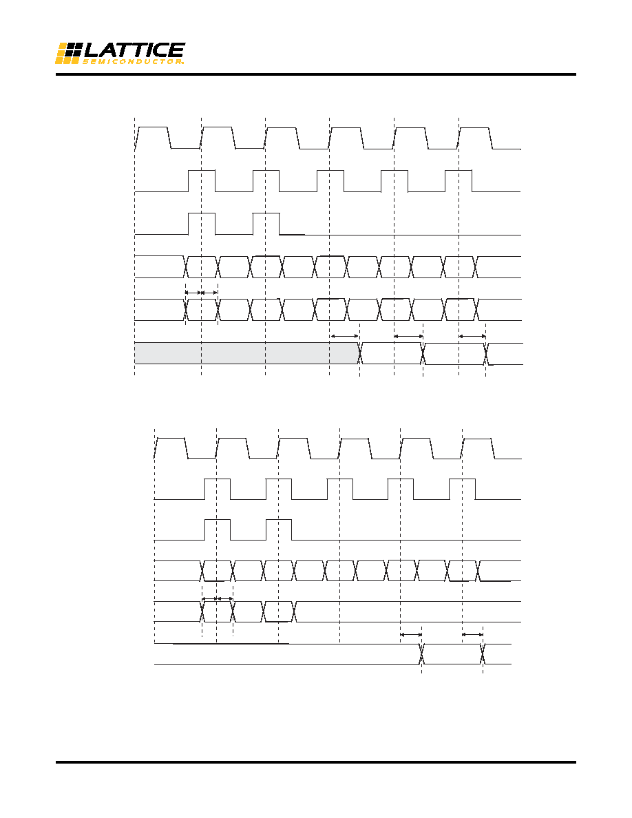
EBR Memory Timing Diagrams
Figure 3-8. Read/Write Mode (Normal)
Note: Input data and address are registered at the positive edge of the clock and output data appears after the positive edge of the clock.
Figure 3-9. Read/Write Mode with Input and Output Registers
A0
A1
A0
A1
D0
D1
DOA
A0
tCO_EBR
tSU tH
D0
D1
D0
DIA
ADA
WEA
CSA
CLKA
A0
A1
A0
D0
D1
output is only updated during a read cycle
A1
D0
D1
Mem(n) data from previous read
DIA
ADA
WEA
CSA
CLKA
DOA (Regs)
tSU tH
tCOO_EBR
相關PDF資料 |
PDF描述 |
|---|---|
| A562K20X7RL5UAA | CAP CER 5600PF 500V X7R AXIAL |
| T491X106M050AT | CAP TANT 10UF 50V 20% 2917 |
| TPSD227M006R0125 | CAP TANT 220UF 6.3V 20% 2917 |
| VI-B3Z-CY-S | CONVERTER MOD DC/DC 2V 20W |
| VI-B3Z-CX-S | CONVERTER MOD DC/DC 2V 30W |
相關代理商/技術參數(shù) |
參數(shù)描述 |
|---|---|
| LFEC20E-5F484I | 制造商:LATTICE 制造商全稱:Lattice Semiconductor 功能描述:LatticeECP/EC Family Data Sheet |
| LFEC20E-5F672C | 功能描述:FPGA - 現(xiàn)場可編程門陣列 19.7 LUT 496 I/O RoHS:否 制造商:Altera Corporation 系列:Cyclone V E 柵極數(shù)量: 邏輯塊數(shù)量:943 內(nèi)嵌式塊RAM - EBR:1956 kbit 輸入/輸出端數(shù)量:128 最大工作頻率:800 MHz 工作電源電壓:1.1 V 最大工作溫度:+ 70 C 安裝風格:SMD/SMT 封裝 / 箱體:FBGA-256 |
| LFEC20E-5F672I | 制造商:LATTICE 制造商全稱:Lattice Semiconductor 功能描述:LatticeECP/EC Family Data Sheet |
| LFEC20E-5F900C | 制造商:LATTICE 制造商全稱:Lattice Semiconductor 功能描述:LatticeECP/EC Family Data Sheet |
| LFEC20E-5F900I | 制造商:LATTICE 制造商全稱:Lattice Semiconductor 功能描述:LatticeECP/EC Family Data Sheet |
發(fā)布緊急采購,3分鐘左右您將得到回復。