- 您現(xiàn)在的位置:買賣IC網(wǎng) > PDF目錄4567 > LFECP33E-3FN672C (Lattice Semiconductor Corporation)IC FPGA 32.8KLUTS 496I/O 672-BGA PDF資料下載
參數(shù)資料
| 型號(hào): | LFECP33E-3FN672C |
| 廠商: | Lattice Semiconductor Corporation |
| 文件頁數(shù): | 129/163頁 |
| 文件大小: | 0K |
| 描述: | IC FPGA 32.8KLUTS 496I/O 672-BGA |
| 產(chǎn)品培訓(xùn)模塊: | LatticeECP3 Introduction |
| 標(biāo)準(zhǔn)包裝: | 40 |
| 系列: | ECP |
| 邏輯元件/單元數(shù): | 32800 |
| RAM 位總計(jì): | 434176 |
| 輸入/輸出數(shù): | 496 |
| 電源電壓: | 1.14 V ~ 1.26 V |
| 安裝類型: | 表面貼裝 |
| 工作溫度: | 0°C ~ 85°C |
| 封裝/外殼: | 672-BBGA |
| 供應(yīng)商設(shè)備封裝: | 672-FPBGA(27x27) |
第1頁第2頁第3頁第4頁第5頁第6頁第7頁第8頁第9頁第10頁第11頁第12頁第13頁第14頁第15頁第16頁第17頁第18頁第19頁第20頁第21頁第22頁第23頁第24頁第25頁第26頁第27頁第28頁第29頁第30頁第31頁第32頁第33頁第34頁第35頁第36頁第37頁第38頁第39頁第40頁第41頁第42頁第43頁第44頁第45頁第46頁第47頁第48頁第49頁第50頁第51頁第52頁第53頁第54頁第55頁第56頁第57頁第58頁第59頁第60頁第61頁第62頁第63頁第64頁第65頁第66頁第67頁第68頁第69頁第70頁第71頁第72頁第73頁第74頁第75頁第76頁第77頁第78頁第79頁第80頁第81頁第82頁第83頁第84頁第85頁第86頁第87頁第88頁第89頁第90頁第91頁第92頁第93頁第94頁第95頁第96頁第97頁第98頁第99頁第100頁第101頁第102頁第103頁第104頁第105頁第106頁第107頁第108頁第109頁第110頁第111頁第112頁第113頁第114頁第115頁第116頁第117頁第118頁第119頁第120頁第121頁第122頁第123頁第124頁第125頁第126頁第127頁第128頁當(dāng)前第129頁第130頁第131頁第132頁第133頁第134頁第135頁第136頁第137頁第138頁第139頁第140頁第141頁第142頁第143頁第144頁第145頁第146頁第147頁第148頁第149頁第150頁第151頁第152頁第153頁第154頁第155頁第156頁第157頁第158頁第159頁第160頁第161頁第162頁第163頁
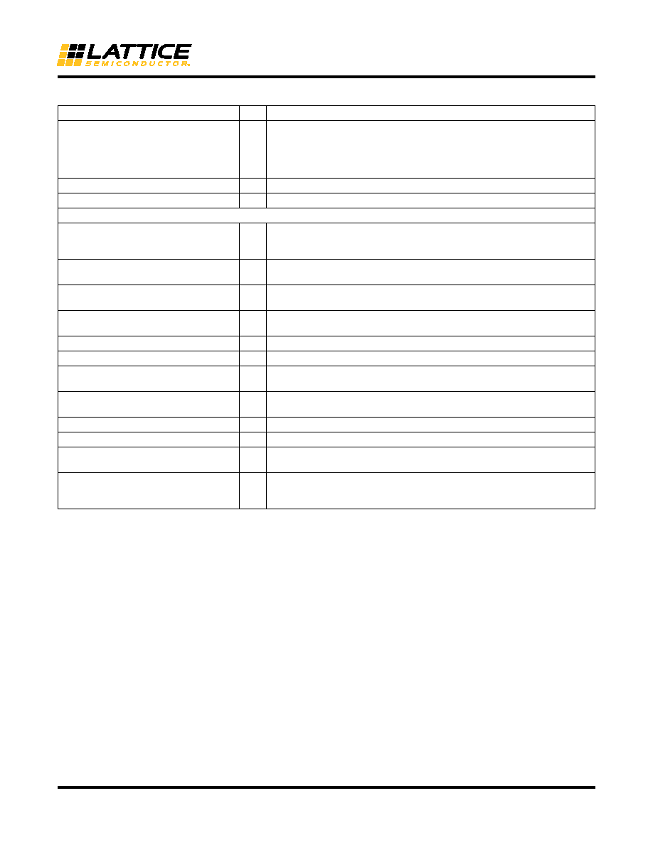
4-2
Pinout Information
LatticeECP/EC Family Data Sheet
TDI
I
Test Data in pin. Used to load data into device using 1149.1 state machine.
After power-up, this TAP port can be activated for configuration by sending
appropriate command. (Note: once a configuration port is selected it is
locked. Another configuration port cannot be selected until the power-up
sequence). Pull-up is enabled during configuration.
TDO
O
Output pin. Test Data out pin used to shift data out of device using 1149.1.
VCCJ
—VCCJ - The power supply pin for JTAG Test Access Port.
Configuration Pads (used during sysCONFIG)
CFG[2:0]
I
Mode pins used to specify configuration modes values latched on rising edge
of INITN. During configuration, a pull-up is enabled. These are dedicated
pins.
INITN
I/O
Open Drain pin. Indicates the FPGA is ready to be configured. During config-
uration, a pull-up is enabled. It is a dedicated pin.
PROGRAMN
I
Initiates configuration sequence when asserted low. This pin always has an
active pull-up. This is a dedicated pin.
DONE
I/O
Open Drain pin. Indicates that the configuration sequence is complete, and
the startup sequence is in progress. This is a dedicated pin.
CCLK
I/O
Configuration Clock for configuring an FPGA in sysCONFIG mode.
BUSY/SISPI
I/O
Read control command in SPI3 or SPIX mode.
CSN
I
sysCONFIG chip select (Active low). During configuration, a pull-up is
enabled.
CS1N
I
sysCONFIG chip select (Active low). During configuration, a pull-up is
enabled.
WRITEN
I
Write Data on Parallel port (Active low).
D[7:0]/SPID[0:7]
I/O
sysCONFIG Port Data I/O.
DOUT/CSON
O
Output for serial configuration data (rising edge of CCLK) when using sys-
CONFIG port.
DI/CSSPIN
I/O
Input for serial configuration data (clocked with CCLK) when using sysCON-
FIG port. During configuration, a pull-up is enabled. Output when used in
SPI/SPIX modes.
Signal Descriptions (Cont.)
Signal Name
I/O
Description
相關(guān)PDF資料 |
PDF描述 |
|---|---|
| ABB75DHRD | CONN CARD EXTEND 150POS .050" |
| ACB70DHLT | CONN EDGECARD 140PS .050 DIP SLD |
| ABB70DHLT | CONN EDGECARD 140PS .050 DIP SLD |
| ACB64DHFR | CONN EDGECARD 128POS .050 SMD |
| ABB64DHFR | CONN EDGECARD 128POS .050 SMD |
相關(guān)代理商/技術(shù)參數(shù) |
參數(shù)描述 |
|---|---|
| LFECP33E-3FN672I | 功能描述:FPGA - 現(xiàn)場可編程門陣列 32.8K LUTs 496 I/O RoHS:否 制造商:Altera Corporation 系列:Cyclone V E 柵極數(shù)量: 邏輯塊數(shù)量:943 內(nèi)嵌式塊RAM - EBR:1956 kbit 輸入/輸出端數(shù)量:128 最大工作頻率:800 MHz 工作電源電壓:1.1 V 最大工作溫度:+ 70 C 安裝風(fēng)格:SMD/SMT 封裝 / 箱體:FBGA-256 |
| LFECP33E-3Q208C | 制造商:LATTICE 制造商全稱:Lattice Semiconductor 功能描述:LatticeECP/EC Family Data Sheet |
| LFECP33E-3Q208I | 制造商:LATTICE 制造商全稱:Lattice Semiconductor 功能描述:LatticeECP/EC Family Data Sheet |
| LFECP33E-3QN208C | 制造商:LATTICE 制造商全稱:Lattice Semiconductor 功能描述:LatticeECP/EC Family Data Sheet |
| LFECP33E-3QN208I | 制造商:LATTICE 制造商全稱:Lattice Semiconductor 功能描述:LatticeECP/EC Family Data Sheet |
發(fā)布緊急采購,3分鐘左右您將得到回復(fù)。