- 您現(xiàn)在的位置:買賣IC網(wǎng) > PDF目錄377630 > LFECP3E-5T144C (Lattice Semiconductor Corporation) Dual uPower Low-Voltage Operational Amplifier 8-SOIC PDF資料下載
參數(shù)資料
| 型號: | LFECP3E-5T144C |
| 廠商: | Lattice Semiconductor Corporation |
| 英文描述: | Dual uPower Low-Voltage Operational Amplifier 8-SOIC |
| 中文描述: | LatticeECP / EC的系列數(shù)據(jù)手冊 |
| 文件頁數(shù): | 10/117頁 |
| 文件大小: | 557K |
| 代理商: | LFECP3E-5T144C |
第1頁第2頁第3頁第4頁第5頁第6頁第7頁第8頁第9頁當前第10頁第11頁第12頁第13頁第14頁第15頁第16頁第17頁第18頁第19頁第20頁第21頁第22頁第23頁第24頁第25頁第26頁第27頁第28頁第29頁第30頁第31頁第32頁第33頁第34頁第35頁第36頁第37頁第38頁第39頁第40頁第41頁第42頁第43頁第44頁第45頁第46頁第47頁第48頁第49頁第50頁第51頁第52頁第53頁第54頁第55頁第56頁第57頁第58頁第59頁第60頁第61頁第62頁第63頁第64頁第65頁第66頁第67頁第68頁第69頁第70頁第71頁第72頁第73頁第74頁第75頁第76頁第77頁第78頁第79頁第80頁第81頁第82頁第83頁第84頁第85頁第86頁第87頁第88頁第89頁第90頁第91頁第92頁第93頁第94頁第95頁第96頁第97頁第98頁第99頁第100頁第101頁第102頁第103頁第104頁第105頁第106頁第107頁第108頁第109頁第110頁第111頁第112頁第113頁第114頁第115頁第116頁第117頁
2-7
Architecture
Lattice Semiconductor
LatticeECP/EC Family Data Sheet
Routing
There are many resources provided in the LatticeECP/EC devices to route signals individually or as busses with
related control signals. The routing resources consist of switching circuitry, buffers and metal interconnect (routing)
segments.
The inter-PFU connections are made with x1 (spans two PFU), x2 (spans three PFU) and x6 (spans seven PFU).
The x1 and x2 connections provide fast and ef
fi
cient connections in horizontal and vertical directions. The x2 and
x6 resources are buffered allowing both short and long connections routing between PFUs.
The ispLEVER design tool takes the output of the synthesis tool and places and routes the design. Generally, the
place and route tool is completely automatic, although an interactive routing editor is available to optimize the
design.
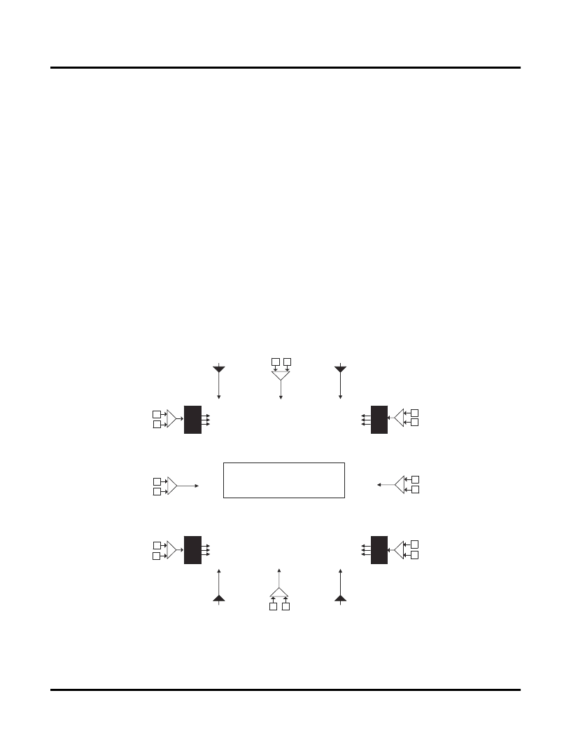
Clock Distribution Network
The clock inputs are selected from external I/O, the sysCLOCK PLLs or routing. These clock inputs are fed
through the chip via a clock distribution system.
Primary Clock Sources
LatticeECP/EC devices derive clocks from three primary sources: PLL outputs, dedicated clock inputs and routing.
LatticeECP/EC devices have two to four sysCLOCK PLLs, located on the left and right sides of the device. There
are four dedicated clock inputs, one on each side of the device. Figure 2-6 shows the 20 primary clock sources.
Figure 2-6. Primary Clock Sources
From Routing
Clock Input
From Routing
PLL Input
Clock Input
PLL Input
PLL Input
Clock Input
PLL Input
From Routing
Clock Input
From Routing
PLL
PLL
PLL
PLL
20 Primary Clock Sources
To Quadrant Clock Selection
Note: Smaller devices have two PLLs.
相關PDF資料 |
PDF描述 |
|---|---|
| LFECP3E-5T144I | LatticeECP/EC Family Data Sheet |
| LFECP40E-3F256C | LatticeECP/EC Family Data Sheet |
| LFECP40E-3F256I | LatticeECP/EC Family Data Sheet |
| LFECP40E-3F484C | Dual uPower Low-Voltage Operational Amplifier 8-PDIP |
| LFECP40E-3F484I | LatticeECP/EC Family Data Sheet |
相關代理商/技術參數(shù) |
參數(shù)描述 |
|---|---|
| LFECP3E-5T144I | 制造商:LATTICE 制造商全稱:Lattice Semiconductor 功能描述:LatticeECP/EC Family Data Sheet |
| LFECP40E-3F256C | 制造商:LATTICE 制造商全稱:Lattice Semiconductor 功能描述:LatticeECP/EC Family Data Sheet |
| LFECP40E-3F256I | 制造商:LATTICE 制造商全稱:Lattice Semiconductor 功能描述:LatticeECP/EC Family Data Sheet |
| LFECP40E-3F484C | 制造商:LATTICE 制造商全稱:Lattice Semiconductor 功能描述:LatticeECP/EC Family Data Sheet |
| LFECP40E-3F484I | 制造商:LATTICE 制造商全稱:Lattice Semiconductor 功能描述:LatticeECP/EC Family Data Sheet |
發(fā)布緊急采購,3分鐘左右您將得到回復。