- 您現(xiàn)在的位置:買賣IC網(wǎng) > PDF目錄21970 > LFX125EB-04F256I (Lattice Semiconductor Corporation)IC FPGA 139K GATES 256-BGA PDF資料下載
參數(shù)資料
| 型號(hào): | LFX125EB-04F256I |
| 廠商: | Lattice Semiconductor Corporation |
| 文件頁數(shù): | 35/119頁 |
| 文件大?。?/td> | 0K |
| 描述: | IC FPGA 139K GATES 256-BGA |
| 標(biāo)準(zhǔn)包裝: | 90 |
| 系列: | ispXPGA® |
| 邏輯元件/單元數(shù): | 1936 |
| RAM 位總計(jì): | 94208 |
| 輸入/輸出數(shù): | 160 |
| 門數(shù): | 139000 |
| 電源電壓: | 2.3 V ~ 3.6 V |
| 安裝類型: | 表面貼裝 |
| 工作溫度: | -40°C ~ 105°C |
| 封裝/外殼: | 256-BGA |
| 供應(yīng)商設(shè)備封裝: | 256-FPBGA(17x17) |
| 其它名稱: | 220-1238 |
第1頁第2頁第3頁第4頁第5頁第6頁第7頁第8頁第9頁第10頁第11頁第12頁第13頁第14頁第15頁第16頁第17頁第18頁第19頁第20頁第21頁第22頁第23頁第24頁第25頁第26頁第27頁第28頁第29頁第30頁第31頁第32頁第33頁第34頁當(dāng)前第35頁第36頁第37頁第38頁第39頁第40頁第41頁第42頁第43頁第44頁第45頁第46頁第47頁第48頁第49頁第50頁第51頁第52頁第53頁第54頁第55頁第56頁第57頁第58頁第59頁第60頁第61頁第62頁第63頁第64頁第65頁第66頁第67頁第68頁第69頁第70頁第71頁第72頁第73頁第74頁第75頁第76頁第77頁第78頁第79頁第80頁第81頁第82頁第83頁第84頁第85頁第86頁第87頁第88頁第89頁第90頁第91頁第92頁第93頁第94頁第95頁第96頁第97頁第98頁第99頁第100頁第101頁第102頁第103頁第104頁第105頁第106頁第107頁第108頁第109頁第110頁第111頁第112頁第113頁第114頁第115頁第116頁第117頁第118頁第119頁
Lattice Semiconductor
ispXPGA Family Data Sheet
18
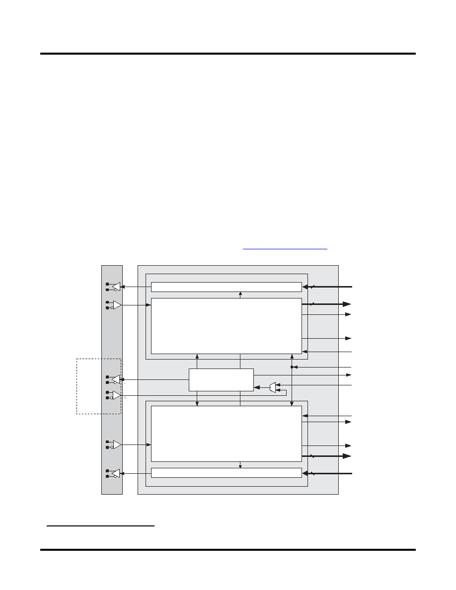
High Speed Serial Interface Block (sysHSI Block)
1
The High Speed Serial Interface (sysHSI) allows high speed serial data transfer over a pair of LVDS I/O. The
ispXPGA devices have multiple sysHSI blocks.
Each sysHSI block has two SERDES blocks which contain two main sub-blocks, Transmitter (with a serializer) and
Receiver (with a deserializer) including Clock/Data Recovery Circuit (CDR). Each SERDES can be used as a full
duplex channel. The two SERDES in sysHSI blocks share a common clock and must operate at the same nominal
frequency. Figure 20 shows the sysHSI block.
Device features support two data coding modes: 10B/12B and 8B/10B (for use with other encoding schemes, see
Lattice’s sysHSI technical notes). The encoding and decoding of the 10B/12B standard are performed within the
sysHSI block. For the 8B/10B standard, the symbol boundaries are aligned internally but the encoding and decod-
ing are performed outside the sysHSI block.
Each SERDES block receives a single high speed serial data input stream (with embedded clock) from an input,
and provide a low speed 10-bit wide data stream and a recovered clock to the device. For transmitting, SERDES
converts a 10-bit wide low-speed data stream to a single high-speed data stream with embedded clock for output.
Additionally, multiple sysHSI blocks can be grouped together to form a source synchronous interface of 1-10 chan-
nels.
For more information on the SERDES/CDR, refer to TN1020, sysHSI Usage Guidelines.
Figure 20. sysHSI Block Diagram
1.
“E-Series” does not support sysHSI.
Shared
Source
Synchronous
Pins
Dr
iv
e
Multiple
sysHSI
b
loc
ks
REFCLK
SOUT
SIN
SS_CLKOUT
SS_CLKIN
SERDES(HSI#A)
CAL
CSLOCK
SERDES(HSI#B)
SOUT
SIN
TXD
RXD
RECCLK
SYDT
10
TXD
RXD
RECCLK
SYDT
10
To PICs
From PICs
From Global
Clock Tree
sysIO
From PICs
To PICs
CDRRST
From PICs
CDRRST
From PICs
Deserializer and Clock/Data Recovery
CSPLL
Serializer
Deserializer and Clock/Data Recovery
SELECT
DEVICES
DISCONTINUED
相關(guān)PDF資料 |
PDF描述 |
|---|---|
| EBC25DCMN-S288 | CONN EDGECARD 50POS .100 EXTEND |
| EBC25DCMH-S288 | CONN EDGECARD 50POS .100 EXTEND |
| GBC05DRYI | CONN EDGECARD 10POS DIP .100 SLD |
| EBC25DCMD-S288 | CONN EDGECARD 50POS .100 EXTEND |
| LFXP15C-4FN256C | IC FPGA 15.5KLUTS 188I/O 256-BGA |
相關(guān)代理商/技術(shù)參數(shù) |
參數(shù)描述 |
|---|---|
| LFX125EB-04F516C | 功能描述:FPGA - 現(xiàn)場(chǎng)可編程門陣列 139K 176 I/O ispJTAG RoHS:否 制造商:Altera Corporation 系列:Cyclone V E 柵極數(shù)量: 邏輯塊數(shù)量:943 內(nèi)嵌式塊RAM - EBR:1956 kbit 輸入/輸出端數(shù)量:128 最大工作頻率:800 MHz 工作電源電壓:1.1 V 最大工作溫度:+ 70 C 安裝風(fēng)格:SMD/SMT 封裝 / 箱體:FBGA-256 |
| LFX125EB-04F516I | 功能描述:FPGA - 現(xiàn)場(chǎng)可編程門陣列 139K 176 I/O ispJTAG RoHS:否 制造商:Altera Corporation 系列:Cyclone V E 柵極數(shù)量: 邏輯塊數(shù)量:943 內(nèi)嵌式塊RAM - EBR:1956 kbit 輸入/輸出端數(shù)量:128 最大工作頻率:800 MHz 工作電源電壓:1.1 V 最大工作溫度:+ 70 C 安裝風(fēng)格:SMD/SMT 封裝 / 箱體:FBGA-256 |
| LFX125EB-04FH516C | 功能描述:FPGA - 現(xiàn)場(chǎng)可編程門陣列 Use LFX125EB-04F516C RoHS:否 制造商:Altera Corporation 系列:Cyclone V E 柵極數(shù)量: 邏輯塊數(shù)量:943 內(nèi)嵌式塊RAM - EBR:1956 kbit 輸入/輸出端數(shù)量:128 最大工作頻率:800 MHz 工作電源電壓:1.1 V 最大工作溫度:+ 70 C 安裝風(fēng)格:SMD/SMT 封裝 / 箱體:FBGA-256 |
| LFX125EB-04FH516I | 功能描述:FPGA - 現(xiàn)場(chǎng)可編程門陣列 Use LFX125EB-04F516I RoHS:否 制造商:Altera Corporation 系列:Cyclone V E 柵極數(shù)量: 邏輯塊數(shù)量:943 內(nèi)嵌式塊RAM - EBR:1956 kbit 輸入/輸出端數(shù)量:128 最大工作頻率:800 MHz 工作電源電壓:1.1 V 最大工作溫度:+ 70 C 安裝風(fēng)格:SMD/SMT 封裝 / 箱體:FBGA-256 |
| LFX125EB-04FN256C | 功能描述:FPGA - 現(xiàn)場(chǎng)可編程門陣列 E-Ser139K Gt ispJTAG 2.5/3.3V -4 Spd RoHS:否 制造商:Altera Corporation 系列:Cyclone V E 柵極數(shù)量: 邏輯塊數(shù)量:943 內(nèi)嵌式塊RAM - EBR:1956 kbit 輸入/輸出端數(shù)量:128 最大工作頻率:800 MHz 工作電源電壓:1.1 V 最大工作溫度:+ 70 C 安裝風(fēng)格:SMD/SMT 封裝 / 箱體:FBGA-256 |
發(fā)布緊急采購,3分鐘左右您將得到回復(fù)。