- 您現(xiàn)在的位置:買賣IC網(wǎng) > PDF目錄30743 > LM1837M (NATIONAL SEMICONDUCTOR CORP) 2 CHANNEL, AUDIO PREAMPLIFIER, PDSO16 PDF資料下載
參數(shù)資料
| 型號(hào): | LM1837M |
| 廠商: | NATIONAL SEMICONDUCTOR CORP |
| 元件分類: | 音頻/視頻放大 |
| 英文描述: | 2 CHANNEL, AUDIO PREAMPLIFIER, PDSO16 |
| 封裝: | DIP-16 |
| 文件頁數(shù): | 11/14頁 |
| 文件大小: | 450K |
| 代理商: | LM1837M |

External Components (Figure 1)
Component Normal Range of Value and Function
R1 C2
2 kX –40 kX 01 mF–10 mF (low leakage)
Set turn-on delay and second amplifier’s low
frequency pole Leakage current in C2 results
in DC offset between the amplifier’s inputs
and therefore this current should be kept low
R1 is set equal to R2 such that any input off-
set voltage due to bias current is effectively
cancelled An input offset voltage is generat-
ed by the input offset current multiplied by
the value of these resistors
R2 R3
2 kX –40 kX 500 kX –10 MX
Sets the DC and low frequency gain of the
output amplifier The total input offset voltage
will also be multiplied by the DC gain of this
amplifier It is therefore essential to keep the
input offset voltage specification in mind
when employing high DC gain in the output
amplifier ie 5 mV c 400 e 2V offset at the
output
R4 C1
10 kX – 200 kX 000047 mF – 001 mF
Set tape playback equalization characteris-
tics in conjunction with R3 (calculations for
the component values are included in the Ap-
plication Hints section)
Component Normal Range of Value and Function
R6
2 kX –47 kX
Biases the output diode when it is used in DC
switching applications This resistor can be
excluded if diode switching is not desired
C3
100 pF – 1000 pF
Often used to resonate with tape head in or-
der to compensate for tape play-back losses
including tape head gap and eddy current
For a typical cassette tape head the reso-
nant frequency selected is usually between
13 kHz and 17 kHz
R5
100 kX –10 MX
Increases the output DC bias voltage from
the nominal 25V value (see Application
Hints)
R7
Optionally used for tape muting The use of
this resistor can also provide ‘‘no-pop’’ turn-
off if desired (see Application Hints)
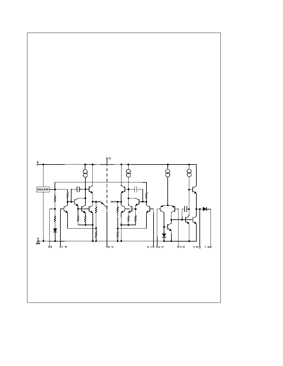
Simplified Schematic
TLH7902 – 9
6
Obsolete
相關(guān)PDF資料 |
PDF描述 |
|---|---|
| LM1851N | POWER SUPPLY SUPPORT CKT, PDIP8 |
| LM1851M | POWER SUPPLY SUPPORT CKT, PDSO8 |
| LM1865MX | FM, AUDIO DEMODULATOR, PDSO20 |
| LM1875DWF | 25 W, 1 CHANNEL, AUDIO AMPLIFIER, UUC |
| LM1875LB02 | 25 W, 1 CHANNEL, AUDIO AMPLIFIER, PZFM5 |
相關(guān)代理商/技術(shù)參數(shù) |
參數(shù)描述 |
|---|---|
| LM1837N | 制造商:NSC 制造商全稱:National Semiconductor 功能描述:Low Noise PREAMPLIFIER FOR AUTOREVERSING TAPE PLAYBACK SYSTEMS |
| LM1837N/A+ | 制造商:未知廠家 制造商全稱:未知廠家 功能描述:Preamp/Equalizer for Audio Tape Recorder |
| LM1837N/B+ | 制造商:未知廠家 制造商全稱:未知廠家 功能描述:Preamp/Equalizer for Audio Tape Recorder |
| LM185 | 制造商:Texas Instruments 功能描述: |
| LM185_08 | 制造商:NSC 制造商全稱:National Semiconductor 功能描述:Adjustable Micropower Voltage References |
發(fā)布緊急采購,3分鐘左右您將得到回復(fù)。